[Source: "High-tech LED - Technology and Applications" October issue]
I. Introduction
In order to completely replace traditional light sources such as incandescent lamps and energy-saving lamps in the field of lighting, in addition to efforts to reduce production costs, LEDs need to further improve electro-optic efficiency and reduce the heat generation of chips to effectively improve the service life and reliability of LEDs. [1]. The main reason for the low light extraction efficiency or external quantum efficiency of LEDs is that the difference in refractive index between the surface material of the LED and the air is so great that the light emitted from the active area of ​​the LED is totally reflected at the interface and cannot be emitted [2]. At present, several methods for improving the efficiency of LED light extraction have appeared in the world, such as surface roughening technology, introducing a Bragg reflection layer inside the LED, and fabricating a photonic crystal structure on the surface of the substrate or the LED [3]. The photonic crystal structure is introduced into a common LED device, and the photon band gap effect peculiar to the photonic crystal can enhance the spontaneous emission of light in a direction perpendicular to the surface of the LED, thereby significantly improving the light extraction efficiency of the LED [4]. Fan et al. [5] theoretically studied the effect of two-dimensional photonic crystal plate structure on changing the spatial distribution of spontaneous emission intensity of LED, and proved that two-dimensional photonic crystal can effectively improve the light extraction efficiency of LED.
On the other hand, some research groups at home and abroad have used different fabrication processes to prepare gallium nitride-based LEDs with photonic crystal structures, and actually observed a significant increase in LED light extraction efficiency. Lin et al. used electron beam lithography to fabricate the world's first LED device with a photonic crystal structure. The results of the study show that an LED with a photonic crystal structure has an output power 2.3 times higher than that of an ordinary LED without a photonic crystal structure. Ba Kui et al. used nanoimprint technology to fabricate a blue gallium nitride-based LED with a photonic crystal structure, which also achieved excellent results in increasing the optical output power of the LED by 60%. Kim et al. used a laser holographic interferometry method to create a square-arranged photonic crystal structure on the surface transparent electrode layer (ITO) of a gallium nitride-based LED, and achieved an amazing result of increasing the light extraction efficiency of the LED by 2.1 times. . Because laser holographic interference technology has the advantages of convenient, fast and low-cost production of large-area photonic crystal patterns, it is more suitable for industrial production than electron beam etching or nanoimprinting. Figure 1 is a schematic illustration of a gallium nitride-based LED having a photonic crystal structure prepared on the surface of an ITO.
Second, photonic crystal and its working principle to improve LED light extraction efficiency
In 1987, Yablonovitch and John borrowed the concept of semiconductor crystals and their electronic band gaps, and for the first time independently proposed the concept of photonic crystals. Photonic crystals are structures that are periodically arranged in space by dielectric materials having different dielectric constants. When light waves propagate in it, the principles of refraction, reflection, and transmission are followed, just as electrons are periodically disturbed by atoms in the crystal to form an electron band structure, and photons are modulated by Bragg scattering of a medium whose refractive index changes periodically. Thereby forming a photonic band structure. In the photonic energy band of a photonic crystal, a frequency region in which light waves of certain frequencies are completely impermeable may be present. This frequency region is called a photonic band gap or a photonic band gap.
Unfinished
For more information, please refer to the October issue of "High-tech LED-Technology and Applications"
I. Introduction
In order to completely replace traditional light sources such as incandescent lamps and energy-saving lamps in the field of lighting, in addition to efforts to reduce production costs, LEDs need to further improve electro-optic efficiency and reduce the heat generation of chips to effectively improve the service life and reliability of LEDs. [1]. The main reason for the low light extraction efficiency or external quantum efficiency of LEDs is that the difference in refractive index between the surface material of the LED and the air is so great that the light emitted from the active area of ​​the LED is totally reflected at the interface and cannot be emitted [2]. At present, several methods for improving the efficiency of LED light extraction have appeared in the world, such as surface roughening technology, introducing a Bragg reflection layer inside the LED, and fabricating a photonic crystal structure on the surface of the substrate or the LED [3]. The photonic crystal structure is introduced into a common LED device, and the photon band gap effect peculiar to the photonic crystal can enhance the spontaneous emission of light in a direction perpendicular to the surface of the LED, thereby significantly improving the light extraction efficiency of the LED [4]. Fan et al. [5] theoretically studied the effect of two-dimensional photonic crystal plate structure on changing the spatial distribution of spontaneous emission intensity of LED, and proved that two-dimensional photonic crystal can effectively improve the light extraction efficiency of LED.
On the other hand, some research groups at home and abroad have used different fabrication processes to prepare gallium nitride-based LEDs with photonic crystal structures, and actually observed a significant increase in LED light extraction efficiency. Lin et al. used electron beam lithography to fabricate the world's first LED device with a photonic crystal structure. The results of the study show that an LED with a photonic crystal structure has an output power 2.3 times higher than that of an ordinary LED without a photonic crystal structure. Ba Kui et al. used nanoimprint technology to fabricate a blue gallium nitride-based LED with a photonic crystal structure, which also achieved excellent results in increasing the optical output power of the LED by 60%. Kim et al. used a laser holographic interferometry method to create a square-arranged photonic crystal structure on the surface transparent electrode layer (ITO) of a gallium nitride-based LED, and achieved an amazing result of increasing the light extraction efficiency of the LED by 2.1 times. . Because laser holographic interference technology has the advantages of convenient, fast and low-cost production of large-area photonic crystal patterns, it is more suitable for industrial production than electron beam etching or nanoimprinting. Figure 1 is a schematic illustration of a gallium nitride-based LED having a photonic crystal structure prepared on the surface of an ITO.
Second, photonic crystal and its working principle to improve LED light extraction efficiency
In 1987, Yablonovitch and John borrowed the concept of semiconductor crystals and their electronic band gaps, and for the first time independently proposed the concept of photonic crystals. Photonic crystals are structures that are periodically arranged in space by dielectric materials having different dielectric constants. When light waves propagate in it, the principles of refraction, reflection, and transmission are followed, just as electrons are periodically disturbed by atoms in the crystal to form an electron band structure, and photons are modulated by Bragg scattering of a medium whose refractive index changes periodically. Thereby forming a photonic band structure. In the photonic energy band of a photonic crystal, a frequency region in which light waves of certain frequencies are completely impermeable may be present. This frequency region is called a photonic band gap or a photonic band gap.
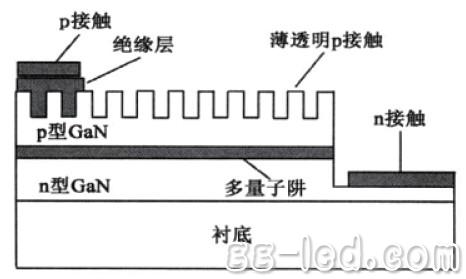
Figure 1 Schematic diagram of a gallium nitride-based LED having a photonic crystal structure
Unfinished
For more information, please refer to the October issue of "High-tech LED-Technology and Applications"
Diode Module is called silicon stack, it is made from several diodes in series, the number of the diode is by its highest pressure (maximum) negative peak pressure, main purpose is for high voltage rectifier. China Diode Module,High Voltage Diodes supplier & manufacturer, offer low price, high quality Caterpillar Diode Module,High Frequency Diode Module, etc.
Diode Module
Diode Module,High Voltage Diodes,Caterpillar Diode Module,High Frequency Diode Module
YANGZHOU POSITIONING TECH CO., LTD. , https://www.yzpst.com