Hardware Design of GPS / DR Integrated Navigation System Based on DSP
In response to the needs of the development of low-cost integrated navigation technology, combined with the characteristics of the main sensors, this article introduces the design of the GPS / DR integrated navigation system using floating-point DSPTMS320VC33 as the core processor of the integrated navigation algorithm and the use of TL16C554 for communication port expansion. The design method of system hardware is given. The designed system has the characteristics of small size, low cost, good real-time, high reliability and good scalability, and has a wide range of application value.
0 Preface
At present, the differential GPS horizontal positioning accuracy has reached 3 ~ 5m, which fully meets the requirements of vehicle positioning accuracy. However, because of the GPS signal occlusion problem in the urban high-rise buildings or when crossing overpasses, GPS cannot be located normally. Dead reckoning (DR) is a commonly used vehicle positioning technology, but the direction sensor accumulates a large error over time and cannot be used alone for a long time. The integrated navigation system can use the position and speed information provided by the GPS system to correct and compensate the error of the DR system in real time; when the GPS signal is out of lock, the dead reckoning can be completed through the DR system, which improves the reliability of the integrated navigation system Sex.
In addition to completing a large amount of arithmetic processing work, the integrated navigation system also needs to implement data collection of sensors such as inertial measurement units IMU (gyroscope and accelerometer) and GPS, communication with external systems, sequential logic control, and human-machine interface. In this case, if only one DSP chip is used, the real-time performance of the system is poor, so most combined systems use two or more DSPs or one or several general-purpose microprocessors MPU plus one DSP The scheme that forms the master-slave multiprocessor system. At present, the scheme of combining DSP and FPGA to process high-speed digital signals is more and more widely used.
1 GPS / DR combined navigation system
The GPS / DR combined system has the functions of receiving and processing odometer information, electronic compass information, inertial measurement unit IMU and GPS information. The main block diagram of its system composition is shown in Figure 1.
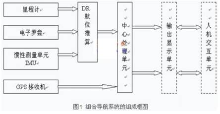
The absolute position information provided by GPS can provide DR with the initial value of estimated positioning and error correction; on the other hand, the DR estimated result can be used to compensate for some random errors in GPS positioning, thereby smoothing the positioning trajectory. Therefore, by combining the two systems with appropriate methods and making full use of the complementarity of their positioning information, it is possible to obtain higher positioning accuracy and reliability than when using either method alone [1].
2 Composition of the central processing unit
At present, the navigation system has developed into a combined navigation system that uses multi-sensor data fusion. The navigation computer must perform a large amount of data communication while completing complex calculations. Therefore, it must have a rich communication interface to complete the task of sensor data collection and transmission. This requires the central processing unit to be able to communicate with the outside while ensuring calculation accuracy and speed.
Through functional analysis of the system, the navigation computer needs to complete data collection, data processing, and data output functions. The data input part mainly completes the collection of various sensor output data; the data processing part mainly completes data filtering, error compensation and initial alignment of micro inertial measurement elements, Kalman filtering, and navigation parameter calculation, etc .; the data output part is mainly responsible for The navigation parameter output is used for positioning navigation or the input required in the next step.
Due to the use of multiple sensors for information fusion, more peripheral communication interfaces are required. At the same time, the external sensor data output communication is mainly carried out through the asynchronous serial communication port that meets the RS-232 standard. If it is directly connected to the central processor, a large number of interruptions The response will definitely affect the processing speed of the CPU. At present, the serial port resources that various MCUs and MPUs can provide are also limited.
Many of the traditional designs use PC104 as the central processor of the system. PC104 is large and expensive, which is not conducive to the miniaturization, low power consumption and low cost of the system. Therefore, this design considers the design of DSP + FPGA + TL16C554, in which DSP completes the calculation of the main navigation parameters, uses TL16C554 to expand the external communication interface, FPGA completes the simulation of the serial port and the corresponding logic control to ensure the three The high-speed communication of the data line improves the system's operating efficiency and calculation accuracy.
The core processor of the central processing unit has to complete large-scale matrix operations and algebraic operations, so the system uses floating-point DSP chip TMS320VC33. The chip has an operation speed of 150MFLOPS and 75MIPS, and a single instruction cycle of 13ns. TMS320VC33 improves speed by improving hardware functions, while other processors increase speed by improving software functions or encoding rates. This way of improving performance through hardware is not possible with single-chip DSPs in the past. The processor has the powerful function of performing parallel multiplication arithmetic operations on integer and floating-point data in a single cycle. At the same time, the chip has the characteristics of low power consumption and low cost, which meets the design requirements of the system [2].
FPGA has programmable features, can easily complete the logic function we need. Use FPGA to expand the peripheral communication interface, mainly to expand the serial communication port of TTL level as the backup of the system. According to the resource requirements for the completion of serial communication and future expansion considerations, ACEX1K30 (hereinafter referred to as ep1k30) of ALTERA is used to complete this work. ep1k30 can provide 119,000 gates of resources, has 1728 logic macro units, can realize the UART serial port, and can also complete the corresponding decoding, logic control and other functions [3].
The system contains multiple sensors, which requires the processor to extend multiple serial ports. The DSP chip TMS320VC33 itself has a serial communication port. If the serial port resources on the DSP chip are used for serial communication directly, it is only suitable for occasions where the transmission data is relatively small and the transmission rate is slow. It takes a lot of system resources and affects the real-time processing function of the sensor. Therefore, this system uses the 4-channel asynchronous transceiver integrated chip TL16C554 produced by TI to extend the DSP serial port to realize the communication between the sensor and the navigation computer. The chip is a kind of serial asynchronous communication.
The large-scale integrated circuit chip of the interface can realize the data parallel / serial and serial / parallel conversion functions. It has a 16-byte FIFO buffer inside. In FIFO mode, the data is buffered into 16-byte data packets before transmission and reception, reducing the number of CPU interrupts. It contains four improved 16C550 asynchronous transmission devices, making serial I / O more reliable [5].
The block diagram of the overall hardware design of the central processing unit is shown in Figure 2.
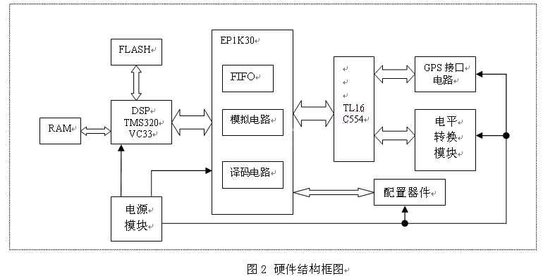
The system makes full use of the advantages of DSP for addition and multiplication operations, and realizes real-time calculation of navigation parameters, and uses FPGA and 16C554 to expand the peripheral communication interface, converts serial data into parallel data, and communicates with DSP through the data bus to process The device is relieved from the burden of a large number of I / O interrupt responses, and improves the operating efficiency of the CPU. The resolved navigation parameters are converted to FPGA through the data bus and output in serial data format. At the same time, considering the large amount of IMU data and the data update rate greater than 100Hz, instead of sending each packet of data directly to the DSP, it first filters the data and then temporarily stores the data through a FIFO. When the amount of data reaches a certain level, the DSP is notified to remove the data, which can further reduce the burden on the DSP and improve the operating efficiency.
3Hardware design of central processing unit
The hardware part of the central processing unit is mainly composed of power supply module, data communication module, FPGA part, DSP part and so on.
3.1 System power module
The entire system needs to use four voltages of 1.8V, 2.5V, 3.3V and 5V. Among them, DSP needs 1.8V and 3.3V as core power supply and I / O power supply; FPGA needs 2.5V and 3.3V voltage power supply; GPS needs 5V voltage power supply, so the entire system uses 5V voltage power supply. Then through two TI's TPS73HD3XX series chips for voltage conversion, you can obtain the required voltage separately. TPS73HD3XX series chips are dual-channel voltage output conversion chips with very low quiescent current. Even for changing loads, the quiescent current can still remain unchanged in practice.
3.2 Data communication module
The hardware structure of the TL16C554 extended data communication module is shown in Figure 3.
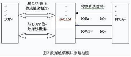
TL16C554's address lines A2 ~ A0, data lines D7 ~ D0 are directly connected to DSP's address bus A2 ~ A0, external data lines D7 ~ D0, and chip select signals CSA ~ CSD, read / write signals IOR / IOW and interrupt signal INTA ~ INTD is connected to FPGA and processed by FPGA. The use of FPGA in the circuit can flexibly configure the address of the UART on the one hand, and can also flexibly generate the strobe and read and write signals of the UART on the other hand, thereby enhancing the flexibility of the system and facilitating system debugging.
3.3 FPGA part
Most of the traditional system design is a multi-machine parallel system that uses DSP as the host for data processing and MCU as the slave for data collection, but the speed limitation of the slave single-chip microcontroller restricts the speed of the entire collection and processing system. In response to this situation, the traditional multi-machine structure is changed to a host-type single machine structure: the system still uses DSP as the data processing host, and replaces the past slave system with pure hardware subsystems composed of various counters, logic circuits, and clock circuits. [4]. However, if the traditional method is used to expand and implement this subsystem with a standard digital circuit chip, multiple circuit chips are inevitably required, which not only complicates the system structure, increases wiring, but also reduces reliability. Therefore, the system uses field programmable gate array device FPGA to design the subsystem. The biggest advantage of designing this system with FPGA is that it saves PCB board area and meets the requirements of low cost. And after the system design is completed, if you want to upgrade and improve the system, you don't have to change any hardware circuits, you only need to reprogram the FPGA internal logic.
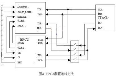
The configuration information cannot be saved after the FPGA is powered off, and it needs to be reconfigured when it is powered on again. Therefore, it is necessary to use an off-chip memory to save the configuration information. In this design, epc2 of ALTERA is selected as the configuration chip. epc2 is a kind of memory with programmable FLASH that can be erased many times, specially used for the configuration of FPGA of ALTERA company. At the same time, the JTAG port on the system board can realize the programming of epc2 and the online configuration of FPGA. The on-line configuration of FPGA and the programming of epc2 are switched through the DIP switch. The specific hardware connection is shown in Figure 4.
3.4 DSP part
DSP requires system algorithm program memory and uses FLASH memory for storage. This system uses four 256k × 16b CY7C1041 to expand two 256k × 32b RAMs to provide storage space for complex combination algorithms; two 16-bit SST39VF400FLASH chips are selected as the system Program memory. The use of FLASH memory overcomes the shortcomings of traditional EPROM, and at the same time helps to reduce the area of ​​the circuit board. Through the DSP emulator, the program can be written into FLASH according to the programming algorithm of FLASH to complete the storage of the DSP algorithm. When the system is powered on, the program can be loaded quickly through the bootstrap method. This can reduce the cost, size and power consumption of the system.
Add a FIFO before the DSP, and wait for the data to be read by the DSP after meeting the requirements, thereby solving the problem of frequent CPU response caused by the large amount of IMU output data. Optimized the efficiency of the system. Each data in the IMU data is composed of high byte and low byte. After receiving the data through the serial port, it can be merged into 16-bit form. The 16C554 chip has a 16-byte FIFO buffer to meet the requirements of the system. Use the half-full signal of the FIFO as an interrupt signal to notify the DSP to receive data and notify the DSP to read. According to the overhead time of the DSP for reading and writing data and the amount of calculations performed, and considering the size of the actual received data and the transmission baud rate, calculate the time spent by the DSP on a packet of data and the cost of writing a packet of data in the FIFO Time, so that the system can successfully complete the solution task.
4 Conclusion
The GPS / DR vehicle combined positioning and navigation system combines the GPS system with the DR system to improve the system's effectiveness, integrity and accuracy. The DR track estimation system can ensure the output of vehicle position information when the satellite signal is lost. The system has the characteristics of all-round, all-weather, unobstructed, high precision, and has good application prospects. This integrated navigation system has powerful data processing capabilities, and has the advantages of small size, low cost, high reliability, and good real-time performance. The design fully utilizes the DSP's powerful data processing capabilities, taking advantage of FPGA's highly integrated programming and simulation convenience, fast speed, etc., and makes the system have great room for improvement in the future, you can use the same hardware to achieve different functions .
100% authentic best 18650 cells, below is our regular inventory list:
authentic sony li ion battery cells
US18650VTC6 3000mAh 15A/20AdischargeUS18650VTC5A 2500mAh 30Adischarge
US18650VTC5 2500mAh 20Adischarge
US18650VTC4 2100mAh 30Adischarge
US18650V3 2200mAh 10Adischarge E bike cells
US18650VC7 3400mAh 5A/8Adischarge
US18650NC1 2900mAh 10Adischarge E bike cells
US454261A8T 1590mAhlipo cells
Original Sanyo cells:
NCR18650BF 3400mAh
NCR18650GA 3450mAh 10AdischargeE bike cells
UR16650ZTA 2500mAh
UR18650ZTA 4.35V 3000mAh
UR18650FJ 2100/2200mAh red top
UR18650FM 2500/2600mAh blue head
UR18650FK 2300/2400mAh green top
UR18650ZY 2450/2550mAh Made In Japan
UR18650ZY 2450/2550mAh
UR18650AY 2150/2250mAh white head
UR14500P 830mah
UR18500F(K) 1620/1700mAh
UR18650NSX 2600mAh 20Adischarge
UF103450PN 1880/2000mAh with fuse
UF103450PN 1880/2000mAh no fuse
UF463450F
UF703450 1430/1480mAh
UF653450 1250/1300mAh
UF624447F 1530mAh
UF553450ZP 1150/1200mAh
UF553450ZP 1150/1200mAh
UF553443ZU 1000mAh
UF463048F
UF553436G
Authentic Panasonic cells:
NCR18650B3 3400mAh
NCR18650A 3100mAh
NCR18650BM 3200mAh
NCR18650 2900mAh
NCR18650PF 2900mAh 10AdischargeE bike cells
NCA103450 2350mAh no breaker
NCA903864 3120mAh
NC-1900SCR
NCR18500A 1940/2040mAh
NCR18650GA 3450mAh 10AdischargeE bike cells
Original Samsung li ion cells:
INR18650-25RM 2500mAh 20Adischarge
INR18650-25RM 2500mAh 20Adischarge
INR18650-25R 2500mAh 20Adischarge,
INR18650-20RM 2000mAh 22Adischarge
INR18650-30Q 3000mAh 15Adischarge
ICR18650-30B 4.35V 3000mAh
INR18650-35E 3500mAh 10Adischarge
INR18650-29E 2900mAh 8.25Adischarge
INR18650-32E 3200mAh 10Adischarge
ICR18650-22P 2150mAh 10Adischarge
ICR18650-22PM 2150mAh 10Adischarge,
ICR18650-22F 2200mAh
ICR18650-22FM 2200mAh
ICR18650-26JM 2600mAh
ICR18650-26FM 2600mAh
ICR18650-26HM 2600mAh
Original LG cells:
INR18650HE4, 2500mAh 20Adischarge
INR18650F1L, 3400mAh
ICR18650S3, 2200mAh,
ICR18650B4/B4L, 2600mAh
ICR18650MF1/MF2,2200mAh,10Adischarge
ICR18650M26,2600mAh, 10Adischarge
INR18650MG1 2900mAh 10Adischarge
INR18650MH1 3200mAh 10Adischarge
INR18650MJ1 3500mAh 10Adischarger
18650 Battery,Best 18650 Battery,18650 Lithium Battery,18650 Lithium Ion Battery
Asarke Industry Co., Limited , https://www.asarke-industry.com