introduction
This wireless system is based on the video communication system of the high-speed radio frequency chip and has an instant shooting function; in the video (continuous) mode, QQVGA resolution is used to transmit video data, which is 160 × 120 (@ 13fps), which can basically achieve real-time video Of the day. In practical applications, the user can view the scene near the (remote) sending end in the LCD of the receiving end. When you see the scene of interest, press the button and wait a moment, you can get a 1.3M pixel image, which is convenient and practical. To simplify the design, the system uses only 8-bit color depth and RGB data format, and does not use a CCD camera chip or FPGA chip for logic control, saving costs.
The following focuses on the wireless video communication system with TMS320VC5402 DSP as the control core, describes the interface design of DSP and camera chip and DSP and radio frequency chip in detail, analyzes the main points in the design, and finally gives some DSP assembly code.
1 Composition and working principle of wireless real-time video system
1.1 Introduction to OV9640 camera chip
OV9640 is a high-performance CM0S image sensor chip launched by the American OmniVision company. It supports 1.3 megapixel image capture and multiple resolutions, including l280 × 960, VGA, QQVGA, CIF, QCIF, etc. and a variety of data output formats, such as Raw RGB , YUV (4: 2: 2), YcbCr (4: 2: 2), etc .; support 8-bit or 16-bit data output; programming it through the SC-CB interface can realize various basic functions of image processing, such as exposure Control, white balance, color saturation, gamma control, etc .; chip voltage requirements are low, can be applied to embedded mobile devices.
1.2 Introduction to nRF24L01 RF chip
nRF24L01 is a single-chip wireless GFSK transceiver chip of Nordic in Norway. It works in the 2.4 to 2.5 GHz ISM frequency band. The maximum wireless transmission rate is 2Mbps. It uses SPI interface to control and data transmission with MCU. Compared with its previous generation product nRF2401, nRF24LOl has better performance and lower power consumption. It can support up to 6 data channels, and each channel supports Enhanced ShockBurst (ESB) technology, with automatic response (AACK) and automatic retransmission (ART) functions, reducing the burden of MCU and reducing the loss of wireless data The packet rate improves the efficiency of two-way transmission. When the ESB is turned on, the nRF24L01 will automatically switch to the receiving mode after the data packet is sent to wait for the other party's response. It will implement automatic retransmission according to the settings of the register.
1.3 System hardware circuit
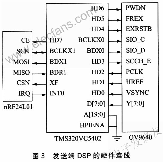
The hardware circuit is composed of two parts: the sending (acquisition) end and the receiving (storage display) end, and realizes the wireless link in the 2.4 GHz frequency band through a high-speed RF chip. The sending end uses TMS320VC5402 DSP as the control core, OV9610 camera chip as the video (or image) acquisition front end, AT29LV1024 Flash ROM as the DSP bootloader storage chip, K4S161622H IMB capacity SDRAM as the program running space and video data buffer, and the video data finally passes The radio frequency chip nRF24LOl is launched; the hardware structure of the receiving end is basically the same as the sending end, and the front end OV9640 can be replaced with the LCD display of the back end. The overall structure block diagram of the entire system is shown in Figure 1.

1.4 System working principle and process
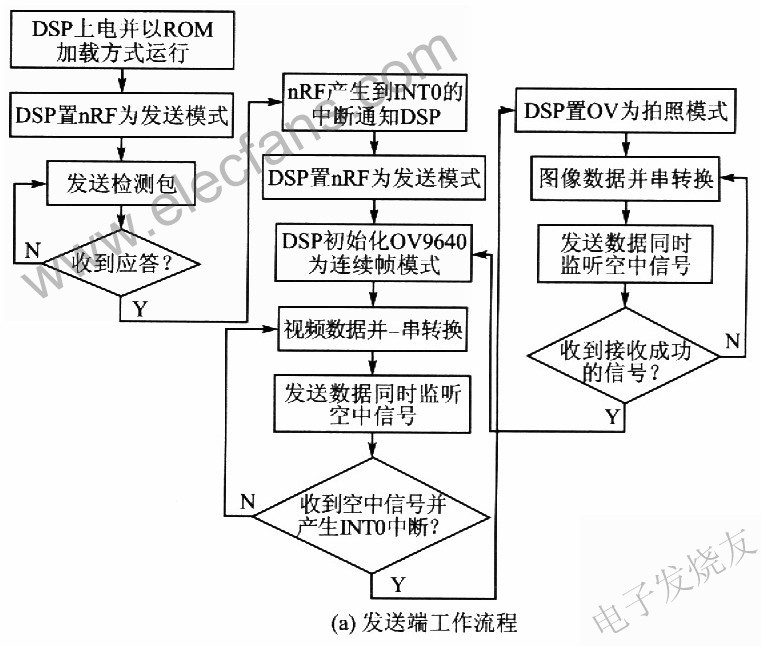
1.4.1 The sender works in video streaming mode
The sending end uses DSP as the core control chip. The DSP is powered on and initialized, and the code in the Flash ROM is loaded into the SDRAM through the BootLoader to achieve high-speed operation of the system to speed up the data processing speed, and the HPI interface is set to general I / O. Then, the nRF24L01 is set to the transmission mode through the McBSPO buffered serial port, and the data packet containing the predetermined address is sent out to occupy the detection receiving end, and the nRF24L01 will automatically switch to the mode of waiting for the response signal. If there is a correct receiving end (address matches), nRF24L01 informs the DSP through INTO interrupt, so that the DSP resets nRF24L01 to send mode, and immediately initializes the OV9640, realizes the SCCB bus through McBSPl buffer serial port, starts the camera and sets For continuous frame mode. The resolution at this time is standard QQVGA, which is 160 × 120 (@ 8bit). Finally, the DSP converts the 8-bit parallel data obtained from D [7: O] into a serial format, and sends it to nRF24L01 through SDRAM buffer and McBSP0. Transmit video data. If the correct receiver is not detected (no INTO interrupt occurs), the DSP will always wait for INTO to occur or until the user turns off the power.
1.4.2 The sender works in shooting mode
In the process of video streaming, nRF24LO1 can simultaneously monitor the air signal and automatically answer. If you receive a photo notification from the receiver (press the button), set the OV9640 to the standard shooting mode with a resolution of l280 × 960 (@ 8bit). Then, DSP sets nRF24L01 as the transmission mode, and sends out the frame data at this time. After sending the image data and waiting for the confirmation signal, the system will return to the video streaming mode. If the reception is unsuccessful, the automatic retransmission function of nRF24LO1 will ensure the integrity of the data transmission.
1.4.3 Workflow at the receiving end
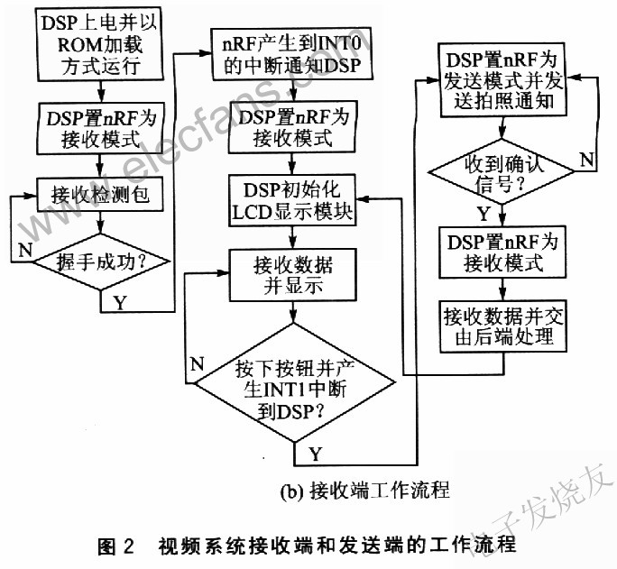
The situation of the power-on initialization of the receiving end is basically the same as that of the sending end, but nRF2dL01 (according to a predetermined address) should be set to the receiving mode to receive the detection signal. After detecting a matching address, the nRF24L01's automatic response function will send a response signal to the sender to confirm the receipt of the signal. At this time, the two parties "handshake" successfully. Next, the DSP is notified by the INTO interrupt, so that the DSP sets the nRF24LO1 to the receiving mode again to receive the continuous video stream from the sending end, and turns on the LCD module to prepare to display the video. Finally, the DSP buffers the video stream through SDRAM and sends it to the LCD display (if other back-end modules such as LCD are parallel interfaces, you need to convert the data into a parallel data format). So far, the system has been able to realize the wireless transmission of real-time video data, and the resolution of the real-time video stream is QQVGA160 × 120 (@ 13fps).
During the display of the video stream, if the user presses the camera button, an INTl interrupt is generated to notify the DSP. The DSP will set nRF24LO1 to the sending mode and send a camera notification signal. After receiving the response signal, nRP24L01 returns to the receiving mode to prepare to receive image data. After receiving, it will automatically send a confirmation signal to indicate the successful reception of image data. Finally, the DSP passes the image data to the back-end module for processing. So far. The system has realized the wireless shooting function of the image, and the photographing effect is 1280 × 960 (@ 1.3 million pixels), which can basically meet the photographing requirements.
The workflow of the receiving end and sending end of the video system is shown in Figure 2.
2 DSP interface design
2.1 Interface design between DSP and OV9640
The chip is controlled by the SCCB bus independently developed by OmniVision and uses three-wire connection. SCCB_E is the serial port enable / disable signal line, and SIO_C and SIO_D are the serial port clock line and data line, respectively. The system only controls the OV9640 without knowing its status, and uses the McBSPO port of the DSP to connect. HD3 is used to open the serial port, and BCLKX0 and HDX0 are used to send clock signals and control data, respectively. The specific hardware connection is shown in Figure 3.
It is worth noting:
â‘ When using the HPI interface of the DSP to connect to the OV9640, in order to obtain signals such as field frequency, line frequency and 8-bit video output, the HPIENA pin of the DSP must be pulled down so that HD [7: 0] can be configured as a general-purpose I / o interface. Realize the start and stop or working mode control of OV9640.
②Set the output size to 1280 × 960 or QQVGA by modifying the OV9640 register COMC.
â‘¢ Modify the register COMH, set the output format to 8-bit RGB format, and set to Master mode.
â‘£FREX is the continuous frame mode enable / disable signal, but the default is disable. The HD4 pin of the DSP should be configured to raise its level, and then use the HD3 to set the EXPSTB pin high to achieve continuous frame data output; set FREX low to return to (single frame) shooting mode.
⑤ Calculate the data transmission rate. The chip outputs parallel 8-bit image signals and vertical and horizontal frequency synchronization signals. The size of the l-frame image (160 × 120) in the video is:
160 × 120 × 8 = 153600 bits / frame
If the maximum transmission speed of nRF24L01 is 2Mbps, it can be transmitted per second
2000000 / 153600≈13 frames
That is, the system can transmit video signals at a speed of 160 × 120 (@ 13 fps).
â‘¥ Parallel conversion of output data.
OV9640 outputs 8-bit parallel data, and nRF24L01 is a serial interface, so parallel data needs to be serialized. The 8-bit parallel data format is HREF, B11, G21, B22, G12 ..., HREF, G21, R22, G23, R24 ... By programming the timing of the sending end and the receiving end, the PCLK, HREF and VSYNC signals obtained from HD [2: 0] can be omitted without being counted as wireless transmission. Therefore, when serializing, the 8-bit data read from D [7: O] each time is put into the SDRAM buffer in order from high bit to low bit, and then sent to nRF24LOl.
2.2 Interface design of DSP and nRF24L01
2.2.1 Design points
DSP uses McBSPl to connect with this chip directly. Among them CSN is SPI chip selection pin, low level is effective, use the XF pin of DSP to connect with CSN pin; CE is the selection pin of transceiver mode, use HD7 to control the high and low level. The connection of other pins is shown in Figure 3. Need to pay attention to when programming:
â‘ Each time before sending a command to nRF24L01 through SPI, the CSN must get a high-to-low level jump
Change, that is, after each instruction is executed, CSN must be set high to continue to send the next instruction.
â‘¡ The SPI of nRF24L01 latches data on the falling edge, so McBSP1 should be configured as "falling edge with delay".
③ The IRQ pin is active low, and every interrupt generated to the DSP must be written “l†to clear.
â‘£If the sending end needs to receive a response, it should configure the data channel O to receive the response signal, and the receiving address (RX_ADDR_PO) should be consistent with the sending address (TX_ADDR).
⑤ The chip must go through Standby mode to enter TX or RX mode, so when switching between TX and RX mode, the CE should be pulled down first to enter Standby mode.
â‘¥ The instruction to write a register can only be executed in Powerdown or Standby mode, so CE should also be pulled low before modifying the register value.
⑦ The following 2.2.2 and 2.2.3 have not enabled the AACK and ART functions. Because the system operates in continuous video streaming mode, it only requires a high data transmission rate to meet real-time performance, and does not require error correction and retransmission. However, in the shooting mode, these two functions should be turned on to ensure the integrity of the image data.
2.2.2 ESB sending data
â‘ Set the configuration bit PRIM_RX low;
â‘¡Keep CSN low and send the address (TX_ADDR) and data (TX_PLD) at the receiving end;
â‘¢ Set CE high and start data transmission;
â‘£ TX_DS interrupt is generated after data transmission is completed;
⑤ Set CE low to enter Standby mode.
2.2.3 ESB receiving data
①The configuration bit PRIM_RX is set high and CE is set high, then after 130μs, nRF24L01 starts to monitor the air signal;
â‘¡ RX_DR generates an interrupt after receiving a legal data packet;
â‘¢ RX_P_NO in the status register records the received data channel;
â‘£ Set CE low to enter Standby mode;
⑤ MCU gets the data through SPI.
2.2.4 Some program examples
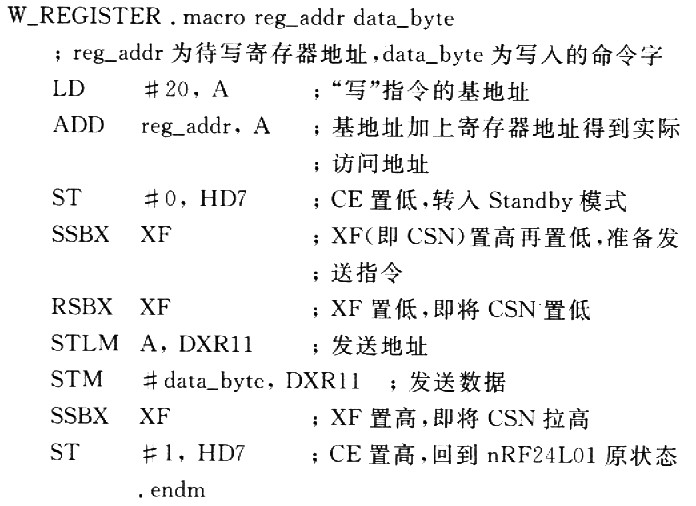
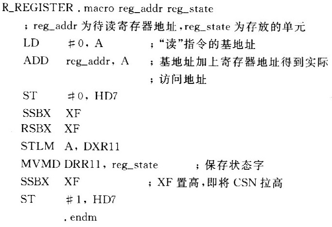
(1) Write nRF24L01 register
(2) Read the nRF24L01 register
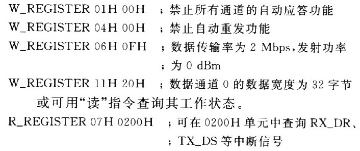
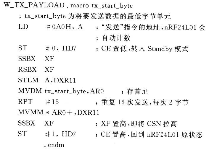
(4) Send data
Assuming that the data width has been set to 32 bytes in (3), W_TX_PAYLOAD.macro tx_start_byte
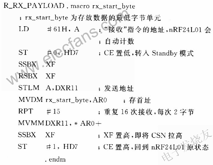
(5) Receive data
Also assume that the data width has been set to 32 bytes in (3), then R_RX_PAYLOAD.macro rx_start_byte
Conclusion
The wireless communication system with DSP as the core uses a high-speed and low-power wireless radio frequency chip nRF24L01, a high-performance TMS320VC5402 digital signal processing chip and a multi-function camera chip OV9640 in its hardware to enable it to achieve powerful video communication functions. And optimize the design at the software level to reduce waiting delay and reduce power consumption. The system is highly scalable. For example, the installation of a voice codec chip can realize the simultaneous transmission of wireless audio and video; the installation of a video compression chip can increase the frame rate; the simultaneous use of two (or more than two) wireless transceiver The chip can achieve full-duplex, which can improve the air data transmission rate; using a high-resolution camera chip can get better video and image effects, but it also increases the difficulty of hardware wiring and software design.
In short, wireless video and wireless image communication are the key development directions in the future wireless field. This design achieves real-time QQVGA video transmission at a certain frame rate, which has certain reference value for the design of similar systems in the future.
To suit the demands of customers as a supplier, wholesaler and trader, we are engaged in offering Battery. Enclosed in polyester tube to stop spillage, these batteries are manufactured with perfection at our vendor's premises. Widely demanded across the nationwide market, these batteries are suitable to use in UPS and inverters.
Battery
Solar Battery,Lead Acid Battery,Rechargeable Battery,Marine Gel Battery
Delight Eco Energy Supplies Co., Ltd. , https://www.cndelight.com