Abstract: Introduce the latest 51 compatible radio frequency SoC (system-on-chip) nRF9E5 system framework, various components, working methods and configuration methods; analyze the structure of the wireless data transmission system and use nRF9E5 to design the communication protocol for wireless data system design; Hardware schematic diagram and program flow chart; summarize the advantages of nRF9E5 in the design of wireless data transmission system.
introduction
nRF9E5 is a system-level RF chip launched by Nordic VLSI on February 5, 2004. It has a built-in nRF905 433/868 / 915MHz transceiver, 8051 compatible microcontroller and 4-input 10-bit 80ksps A / D converter. It is a real System level chip, as shown in Figure 1. The built-in nRF905 transceiver is the same as the transceiver of the nRF905 chip, and can work in the ShockBurst (automatically handle prefix, address and CRC) mode. The built-in voltage adjustment module can suppress the noise to the maximum, provide the system with an operating voltage of 1.9 ~ 3.6V, QFN5 & TImes; 5mm package, carrier detection. nRF9E5 conforms to the relevant standards of the American Communications Commission and the European Telecommunications Standards Institute. Because nRF905 has low power consumption and reliable operation, it is very suitable for the design of wireless data transmission systems.
figure 1
1 nRF9E5 function introduction
1.1 nRF9E5 hardware
(1) Microcontroller
The on-chip microcontroller of nRF9E5 is compatible with the standard 8051, and the instruction timing is slightly different from the standard 8051. The typical difference is that the instruction cycle of the on-chip microcontroller of nRF9E5 is 4 to 20 instruction cycles. The interrupt controller supports 5 extended interrupt sources: ADC interrupt, SPI interrupt, RADIO1 interrupt, RADIO2 interrupt and wake-up timer interrupt. The on-chip controller also has three timers that are the same as 8052. One serial port same as 8051, you can use Timer 1 and Timer 2 as the baud rate generator for asynchronous communication. In addition, 2 data pointers have been expanded to facilitate reading data from the XRAM area. There are 256B of data RAM and 512B of ROM in the microprocessor. After power-on reset or software reset, the processor automatically executes the code in the ROM boot area. The user program is usually loaded into a 4KB RAM from EEROM under the guidance of the boot area. This 4KB RAM can also be used to store data. Most of the NRF9E5 registers are the same as the standard 8051, except that some special function registers are added, such as RADIO (P2), ADCCON, ADCDATAH, ADCDATAL, ADCSTATIC, PWMCON, PWMDUTY, RCAP2L, RCAP2H, CKLFCON, etc. The register addresses of P0, P1 and P2 in nRF9E5 are the same as those in standard 8051, all are 0x80, 0x90, 0xA0, but the functions are different from those in standard 8051. 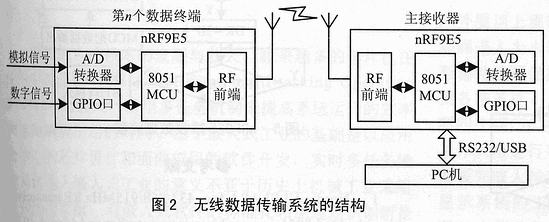
(2) CKLF clock, RTC wake-up timer, GPIO wake-up and WTD
There is a low-frequency clock CKLF in nRF9E5, which is normally open. When the crystal oscillator starts to work, the CKLF frequency is 4 Hz; when the crystal oscillator does not work, CKLF is a low-power RC crystal oscillator, as long as VDD ≥ 1.8V, it works continuously. The RTC wakeup timer, WTD (watchdog) and GPIO wakeup all work at the CKLF frequency to ensure that the chip power consumption can complete these three functions. RTC wake-up timer is a 24-bit programmable down counter, WTD is a 16-bit programmable down counter. RTC wake-up timer and WTD cycle period is generally 300μs ~ 80ms, the default is 1ms. The RTC wake-up timer can also be used as a GPIO output source, that is, when the RTC wake-up timer initialization time overflows, it can generate a program pulse that is used as a GPIO output.
(3) SPI interface and A / D converter
The interface pins of SPI (Serial Peripheral Interface) are MISO (receiving data sent from SDO of EEPROM), SCK (providing clock signal to SCK of EEPROM), MOSI (SDI sending data to EEPROM), EECSN (to EEPROM) The CSN sends an enable signal). The MISO, SCK and MOSI of the SPI port are reused with the lower 3 bits of the P1 port, and the exchange between functions is controlled by the control of the register SPI_CTRL. SPI hardware does not generate any chip select signal, you can use the GPIO port for chip select. Usually, when the system is powered on, the SPI is automatically connected to the off-chip 25320. When the program is loaded, MISO (P1.2) and MOSI (P1.0) may be used for other purposes, such as other SPI devices or GPIO.
The nRF9E5 has a 10-bit ADC. The A / D conversion reference voltage can be set between AREF and 1.22V (internal reference voltage) by software. The four inputs of the A / D converter can be selected by software. Channels 0 to 3 can convert the voltage values ​​on the corresponding pins AIN0 to AIN3 into digital values ​​respectively. Channel 4 is used to monitor the operating voltage of nRF9E5. The A / D converter works in 10-bit mode by default, and it can work in 6-bit, 8-bit or 12-bit mode through software.
image 3
(4) RF transceiver
The nRF9E5 transceiver communicates with other modules through an internal parallel port or an internal SPI port, and has the same functions as the single-chip RF transceiver nRF905. The transceiver communicates with the microcontroller through the parallel port or SPI port of the on-chip MCU. The data is ready, and the carrier detection and address matching signals can be used as the microcontroller and interrupt.
nRF905 works in the 433/868 / 915MHz ISM band. The transceiver consists of a completed frequency synthesizer, a power amplifier, an adjustment Lv and 2 receivers. The output power, channel and other RF parameters can be controlled by programming the special function register RADIO (0xA0). In transmit mode, the RF current consumption is 11 mA, and in receive mode it is 12.5 mA. In order to save energy, the transceiver can be turned on / off through a program.
1.2 nRF9E5 transceiver mode
Unlike nRF401 and nRF903, nRF9E5 uses an SPI interface for data transmission between a microcontroller and a wireless module. This part is completed between the 8051 core in nRF9E5 and nRF905 RF transceiver. It is completed between the 8051 core in nRF9E5 and nRF905 RF transceiver. Completed between the 8051 core in nRF905 and nRF905 RF transceiver. The nRF9E5 transceiver has three working modes, ShockBurst receive (RX) mode, ShockBurst transmit (TX) mode and idle mode. When the transceiver is in idle mode, the microcontroller is still running. 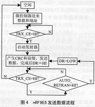
nRF9E5 uses the characteristics of Nordic VLSI's ShockBurst to perform high-speed data transmission. Protocols related to radio frequency data are automatically processed by the nRF9E5 transceiver on-chip. The nRF9E5 can transmit data with the nRF9E5 using only a simple SPI interface. The speed of data transmission depends on the speed of the SPI interface. This can be configured in the nRF9E5 on-chip 8051 core. ShockBurst achieves low-speed data input and high-speed data output, thereby reducing the average energy consumption of the system. In the ShockBurst receiving mode, when a radio frequency packet with a valid address is received, the address matching register bit (AM) and the data ready register bit (DR) notify the on-chip MCU to read the data. In the ShockBurst sending mode, nRF9E5 automatically adds a prefix and CRC check to the data to be sent. When the data is sent, the data ready register bit (DR) will notify the MCU that the data has been processed.
When the system does not send and tasks, it enters idle mode, nRF9E5 in idle mode, once there are tasks to be processed, it can enter ShockBurst receiving mode and ShockBurst sending mode in a short time. In idle mode, the crystal oscillator still works, and the contents of the configuration word will not be lost.
1.3 Carrier detection
In the ShockBurst receiving mode, when the radio frequency carrier in the nRF9E5 working channel appears, the carrier detection pin (CD) is set high, this feature is very good to avoid the collision of different transmitter data packets at the same operating frequency. When the transceiver is ready to transmit data, it first enters the receive mode and detects whether the channel it is working on is idle. The carrier detection standard is generally 5dB lower than the sensitivity. For example, the sensitivity is -100dBm, and the carrier detection function detects carriers as low as -105dBm. In other words, the carrier is lower than -105dBm, the carrier detection signal is low (generally 0), and higher than -95dBm, the carrier detection signal is high (generally VDD), between -105 ~ 95dBm, the carrier detection signal It may be low or high.
2 Wireless data transmission system
2.1 System composition
The wireless data transmission system is somewhat point-to-point, point-to-multipoint and multipoint-to-multipoint. This system is composed of a PC, main receiver and multiple data terminals due to actual application needs. The data transmission before the main receiver and the data terminal is carried out through nRF9E5, forming a point-to-multipoint and multi-wireless data transmission system. In the entire system, the wireless communication between the PC and the data terminal uses the 433MHz frequency band as the carrier frequency. In order to avoid the problem of co-channel interference, the system uses TDMA (TIme Division MulTIple Access) communication technology. The main receiver scans one by one to detect whether each data terminal sends or receives communication requests or other tasks; the data terminal uses an interrupt mode to process the address information sent by the main receiver, and executes the command if it matches the local one. It can be seen that the communication between the upper PC and the data terminal is transformed into the communication between the main receiver and the data terminal, and the communication between the PC and the main receiver through the serial port (USB or UART). The structure of the entire wireless data transmission system is shown in Figure 2.
2.2 Communication protocol
The communication protocol is a rule formulated by both parties to realize the exchange of information. This system uses time division multiple access communication technology (TDMA) to convert point-to-multipoint communication into point-to-point communication. Therefore, it must involve address matching when establishing a communication connection between the source and the sink. Because the communication between the main receiver and the data terminal may be interfered by other data terminals or the external environment and cause errors, a communication protocol is required to ensure the reliability of data transmission.
nRF9E5 has only one protocol format, the prefix is ​​the data, the device address includes the address of the machine and the address of the main receiver, CRC check can be selected 8 or 16 bits.
3 Realization of wireless data transmission system 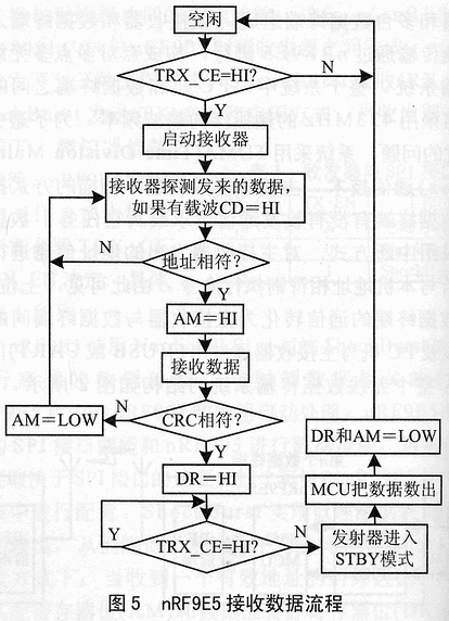
3.1 System hardware
Figure 3 is a hardware schematic diagram of the main receiver in the wireless data transmission system. The hardware principle of the data terminal is similar to Figure 3, except that there is no serial port part connected to the PC, and the GPIO port is connected to the data input terminal corresponding to the A / D conversion slogan, such as a temperature sensor and an interrupt signal. ANT1 and ANT2 are antenna connection pins, PCB loop differential antennas can be used, and the crystal operating frequency is 16MHz. 25AA320 is EEPROM. After nRF9E5 is powered on, the system copies the 25AA320 neutralization program code to the 4KB RAM of nRF9E5 according to the boot program. LM1117 is a power management module that converts 5V levels to 3.3V available for nRF9E5. MAX3232CSE is a level conversion chip for communication between nRF9E5 serial port and PC serial port. It can be seen from Figure 3 that it is very convenient to use nRF9E5 to design a wireless data transmission system. The external dimensions of nRF9E5 are very small, and nRF9E5 is more used in the occasions where the external dimensions are very strict.
3.2 System software
The wireless data transmission is mainly composed of a wireless data terminal, a main receiver and a PC. The serial port is used for communication between the PC and the main receiver. All parts of the entire system serve the purpose of wireless data transmission. Therefore, in the software design of the entire system, wireless data transmission is the most important part. As shown in Figures 4 and 5, it is the process of receiving and sending wireless data transmission. The software design should be based on the communication protocol and consider the error correction of the data. The error detection can use the CRC check 8-bit or 16-bit mode. In Figure 4 and Figure 5, TRX_CE send and receive enable register bit, DR is the data preparation register bit, AM is the address matching register bit, and AUTO_RETRAN is the automatic retransmission register bit.
4 Conclusion
Using the radio frequency wireless system-on-chip nRF9E5, it is easy to realize a small size and high stability wireless data transmission system. The three working frequency bands of 433/868 / 915MHz can be selected according to the needs of use. The nRF9E5 on-chip UART facilitates serial communication with the PC, and its on-chip A / D converter facilitates data acquisition. The nRF9E5's ShockBurst technology and power supervision technology make the power consumption of wireless data transmission systems lower, and there are fewer program codes written in the design to save electricity.
Welding cable is a type of electrical cable that is specifically designed for use in welding applications. It is made up of fine copper strands that are coated with a durable, heat-resistant insulation material. The insulation material is resistant to cuts, tears, abrasions, and other types of damage that can be caused by welding sparks and other hazards.
Welding cable is available in various sizes, ranging from 6 AWG to 4/0 AWG, and is typically sold in lengths of 25 feet or more. The cable is rated for high amperage and voltage, making it suitable for use in welding machines and other heavy-duty electrical equipment.
One of the key benefits of welding cable is its flexibility. The fine copper strands that make up the cable are highly flexible, which makes it easy to maneuver and position in tight spaces. This flexibility also helps to reduce the risk of fatigue and breakage, which can occur with less flexible cables.
Overall, welding cable is an essential component of any welding setup. It provides a reliable and durable electrical connection between the welding machine and the workpiece, helping to ensure safe and efficient welding operations.
Soft Copper Conductor Flexible Core Welding Cable,DC Welding Cable,Flexible Core Conductor Electrical Power Cable,Single Core Copper Welding Wire,Rubber Insulation Electric Welding Cable
Ruitian Cable CO.,LTD. , https://www.rtlinecable.com