The 8051 microcontroller is a widely used 8-bit microprocessor that integrates essential components into a single chip. Here's a detailed overview of its key features and internal structure:
1. **8-bit CPU**: The core of the microcontroller, responsible for executing instructions and performing arithmetic and logic operations.
2. **On-chip Data Memory (RAM)**: Available in 128B or 256B, this memory stores temporary data such as intermediate results, final outputs, and display data. It supports read and write operations for efficient program execution.
3. **On-chip Program Memory (Flash ROM)**: Typically 4KB in size, it stores the program code, constants, and lookup tables. This non-volatile memory allows for reprogramming, making it ideal for embedded applications.
4. **Four 8-bit I/O Ports (P0 to P3)**: These ports can be configured as either input or output interfaces, enabling the microcontroller to interact with external devices like sensors, displays, and actuators.
5. **Timer/Counter Units**: There are two or three timer/counter modules. They can operate in counting mode to track external events or in timing mode to generate precise delays, aiding in real-time control applications.
6. **Full-Duplex UART Serial Port**: This feature enables serial communication between the microcontroller and other devices, facilitating data exchange in systems like modems, computers, and peripheral devices.
7. **Oscillator and Clock Circuit**: An internal oscillator generates the clock signal required for the microcontroller’s operation. However, an external crystal and capacitors are typically connected for higher accuracy and stability.
8. **Interrupt System**: The microcontroller supports five interrupt sources, allowing it to respond to external or internal events without halting the main program flow.
9. **Power-Saving Modes**: Two modes are available—idle and power-down. In idle mode, the CPU stops, but peripherals like RAM, timers, and the serial port continue to function, reducing power consumption by about 85%. In power-down mode, the oscillator stops, and only the RAM contents are preserved until a hardware reset occurs, consuming less than 15 µA.
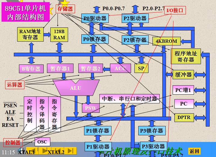
**Structure**
The 8051 microcontroller consists of a central processing unit (CPU), memory (ROM and RAM), and input/output (I/O) interfaces. Its internal architecture is shown in the diagram below.
**Memory Configuration**
The MCS-51 microcontroller has a flexible memory system:
- **On-chip ROM**: 4KB of program memory.
- **On-chip RAM**: 256B of data memory.
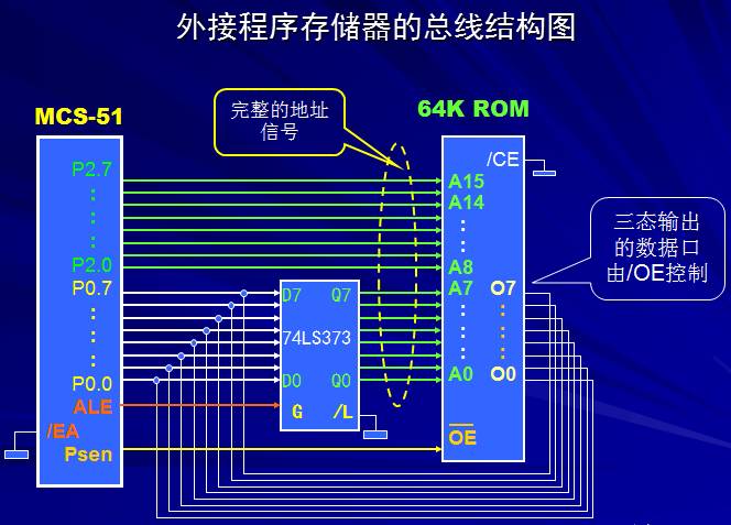
- **External Memory Support**: Up to 64KB of additional program and data memory can be connected externally.
From a physical perspective, the storage system includes on-chip and off-chip ROM and RAM. Logically, it is divided into three spaces:
1. **On-chip Data RAM**
2. **Off-chip Data RAM**
3. **Program Memory (ROM)** – determined by the EA pin level.
When EA = 1, the microcontroller uses the internal 4KB ROM; when EA = 0, it accesses the external ROM. The program always starts at address 0000H, regardless of whether the memory is internal or external.
If the program exceeds 4KB, the microcontroller can either use the external ROM entirely (EA=0) or combine internal and external ROMs (EA=1). In the latter case, the program starts at 1000H in the external ROM.
**Program Memory Special Addresses**
Six specific addresses in the ROM serve as interrupt vector locations:
- **0000H**: Reset vector, where the first instruction is executed.
- **0003H**: External interrupt 0 (INT0).
- **000BH**: Timer 0 overflow interrupt.
- **0013H**: External interrupt 1 (INT1).
- **001BH**: Timer 1 overflow interrupt.
- **0023H**: Serial communication interrupt.
When writing interrupt service routines, these addresses should contain a "jump" instruction to direct the program to the actual interrupt handler.
**First Instruction of the Microcontroller**
The first instruction must be a jump to skip the interrupt vectors and start the main program at 0100H:
```
ORG 0000H
LJMP 0100H
ORG 0100H
START: MOV A, #00H
...
END
```
**External Program Memory**
When using external ROM, set the /EA pin to 0. In this mode, P0 and P2 act as address/data buses, and the /PSEN signal controls the external ROM’s output.
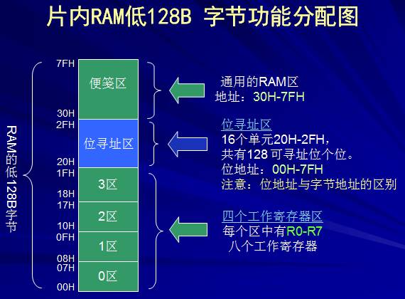
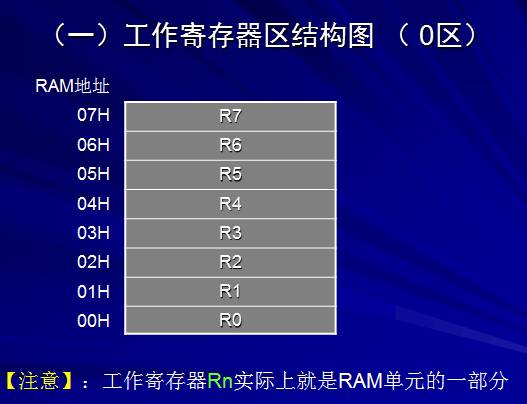
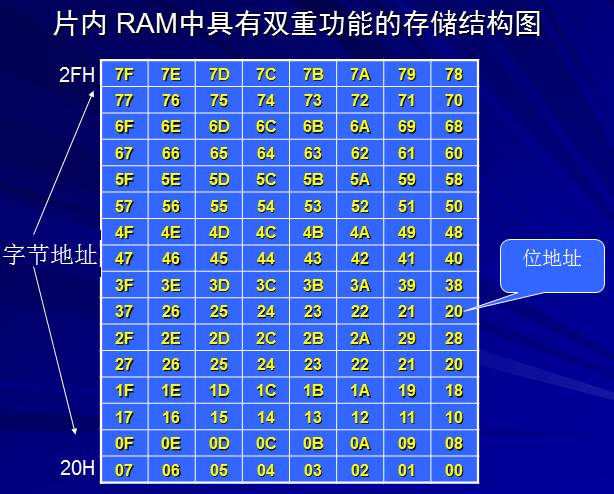
**Internal Data Memory (RAM)**
The internal RAM is divided into two parts: the lower 128 bytes and the upper 128 bytes (SFRs). The lower section includes working registers, bit-addressable memory, and general-purpose storage. The SFR block contains special function registers used to control the microcontroller’s peripherals.
Accessing internal RAM uses the `MOV` instruction, while external RAM requires `MOVX`.

Bang Kng 22000 puffs
Longhua Manxueling Trading Company , https://www.mxlvape.com