The most professional and meticulous dissection, of course, is the iPhone X Depth Map!
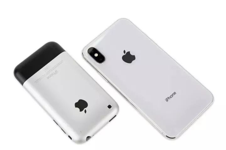
Since it's the tenth anniversary of the iPhone, I thought it would be a great idea to take a photo with the original iPhone. Thanks to Steve Jobs for changing the world forever.
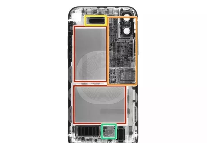
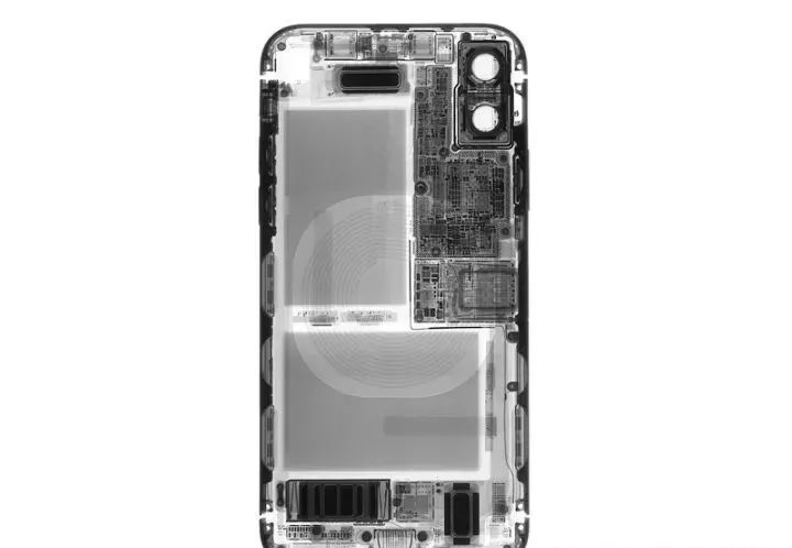
Under X-ray, you can see two batteries (a first in iPhone history), an ultra-small circuit board, and a wireless charging ring. To make space for the Face ID components, the speaker has been slightly moved downward.
There’s also a mysterious chip between the Taptic Engine and the bottom speaker (marked in green). What could it be?

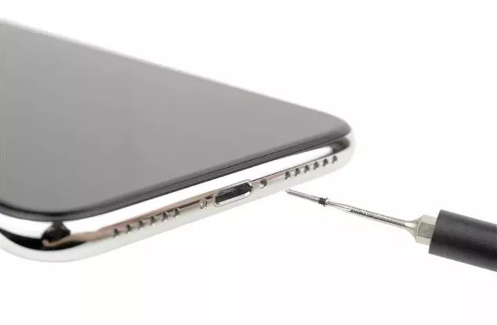
The two screws at the bottom are different from previous models.
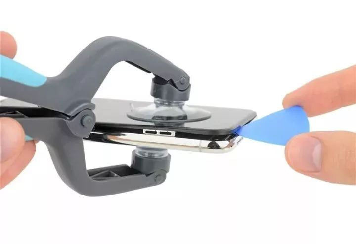
The teardown process is still the same — first, heat it up.
Then separate the screen from the body.
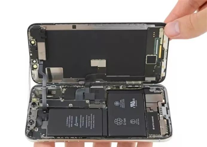
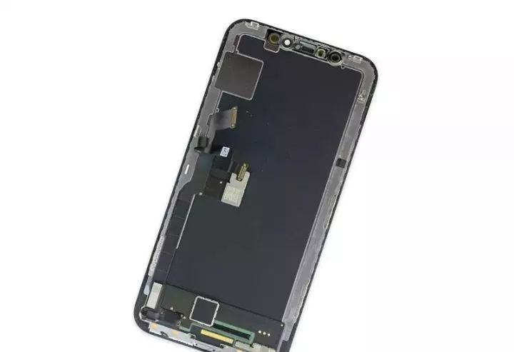
I saw the inner workings, but I had to be careful with the cables.
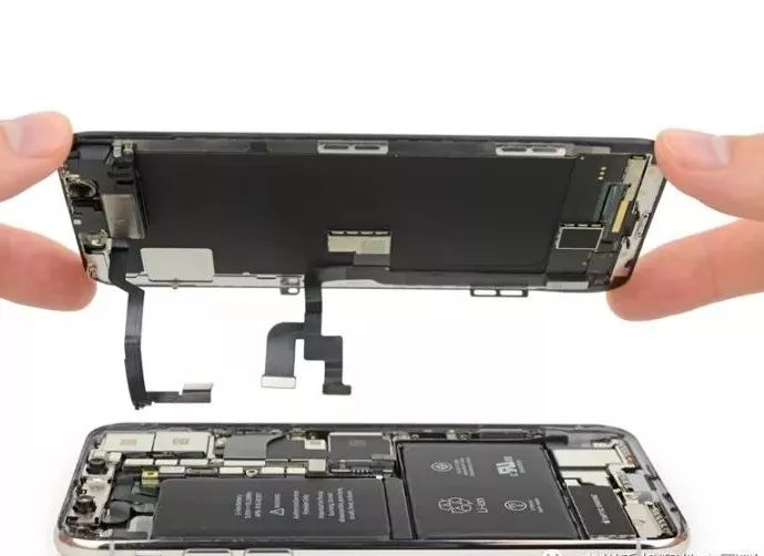
Ok, the front panel is now separated.
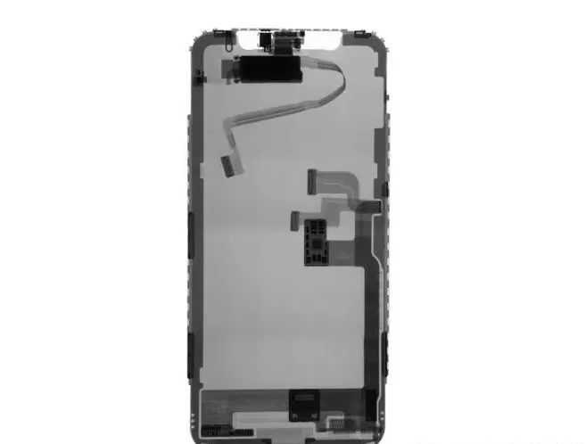
Under X-ray, the front panel shows the mysterious chip that was previously mentioned. It seems to be integrated with the display.
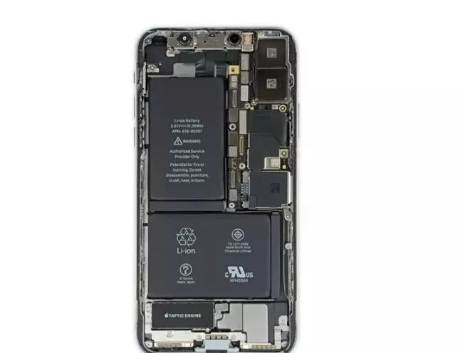
Two batteries occupy most of the internal space.
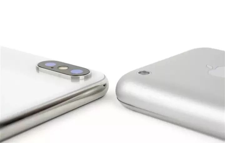
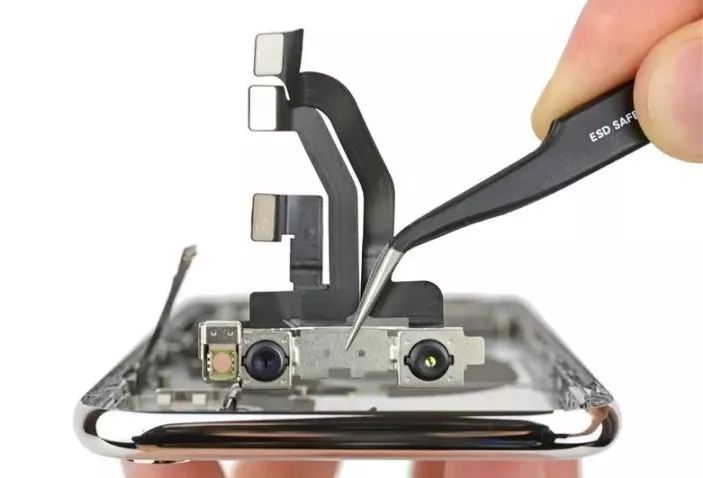
First, remove the dual camera and secure it with a slender metal strip.
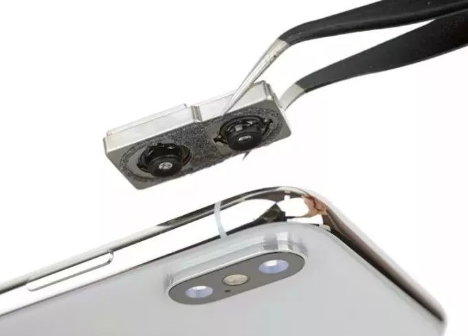
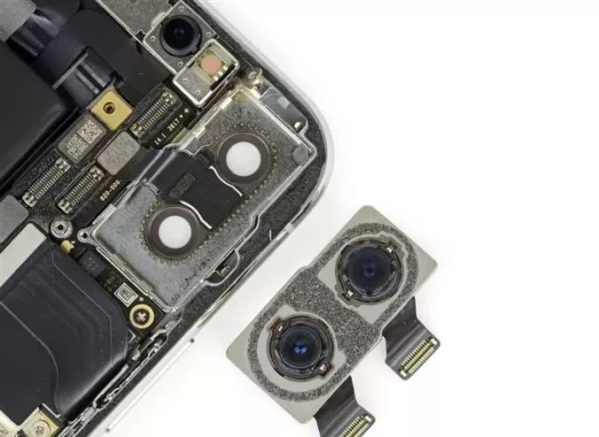
The dual camera module is now removed.
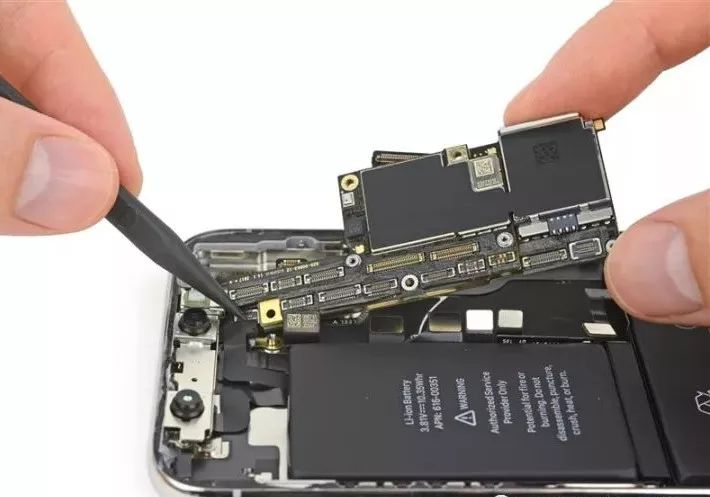
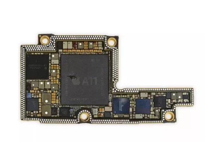
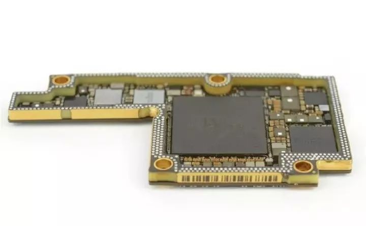
This is the motherboard — is it too small?
The layout of the motherboard is quite dense, showing impressive design capabilities.
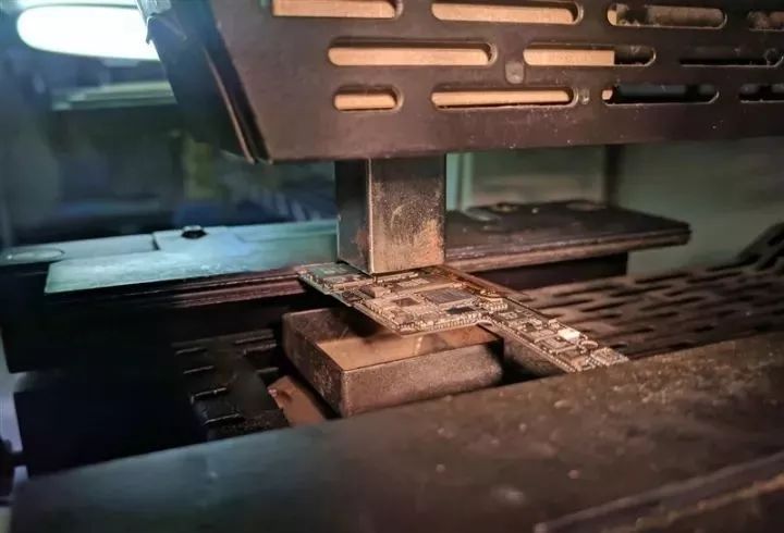
The two layers of the motherboard are tightly welded together and need to be separated using a BGA heat gun.
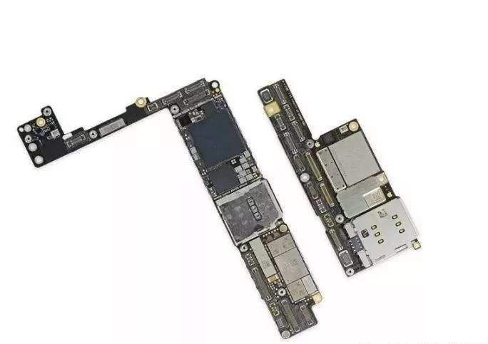
There are three main boards, each varying in size. Compared to the iPhone 8 Plus, the total area is actually 35% larger, but the double-layer stack reduces space usage significantly.
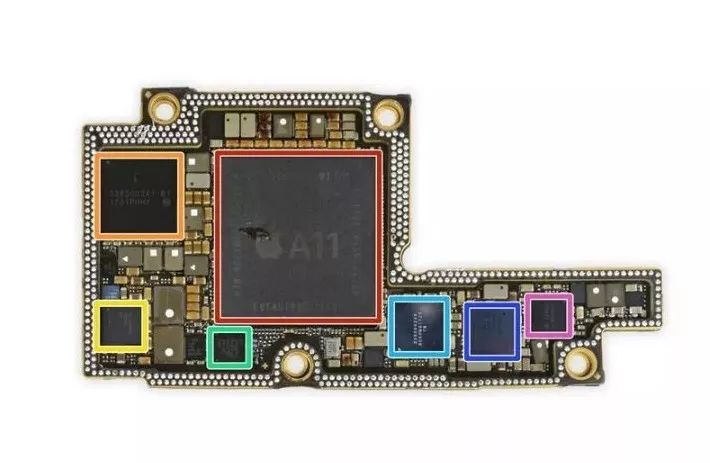
Let’s look at the first board:
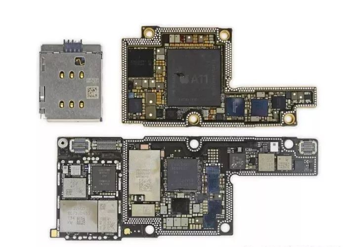
- Red: Apple APL1W72 A11 Bionic processor (with SK Hynix H9HKNNNDBMAUUR 3GB LPDDR4X memory)
- Orange: Apple 338S00341-B1
- Yellow: Texas Instruments 78AVZ81
- Green: NXP 1612A1
- Cyan: Apple 338S00248 audio encoder
- Blue: STB600B0
- Purple: Apple 338S00306 Power Management IC
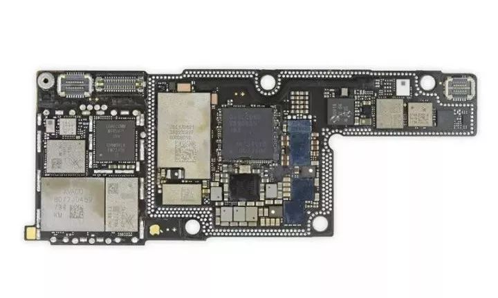
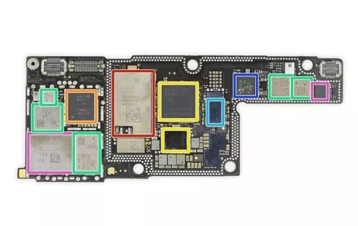
Now, the second board:
- Red: Apple USI 170821 339S00397 Wi-Fi/Bluetooth Module
- Orange: Qualcomm WTR5975 Gigabit LTE Transceiver
- Yellow: Qualcomm MDM9655 Snapdragon X16 LTE baseband, PMD9655 power management IC
- Green: Skyworks 78140-22/SKY77366-17 power amplifier, S770 6662, 3760 5418 1736
- Cyan: Broadcom BCM15951 touch controller
- Blue: NXP 80V18 PN80V NFC Controller
- Purple: Broadcom AFEM-8072, MMMB power amplifier
Next, the last small piece:
- Red: Toshiba TSB3234X68354TWNA1 64GB flash memory
- Orange: Apple/Cirrus Logic 338S00296 Audio Amplifier
Between the multiple boards, Apple uses a series of perforations instead of cables.
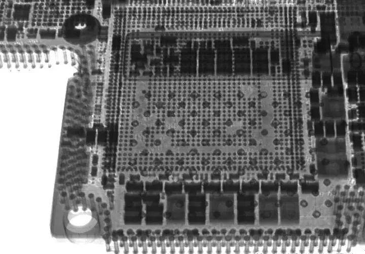
Under X-ray, the 3D structure of the SoC and surrounding circuitry becomes more visible, especially the peripheral perforations.
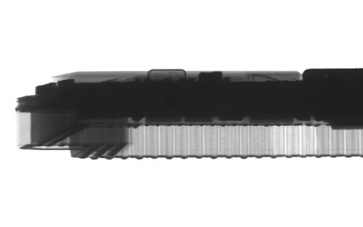
Looking at the side view under X-ray, you can clearly see the perforations.
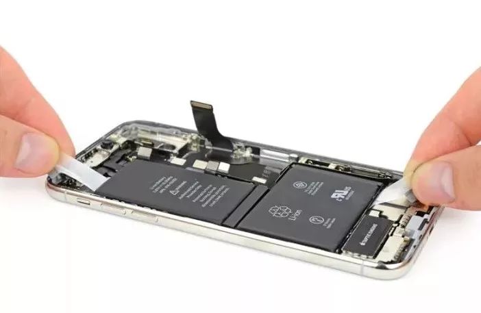
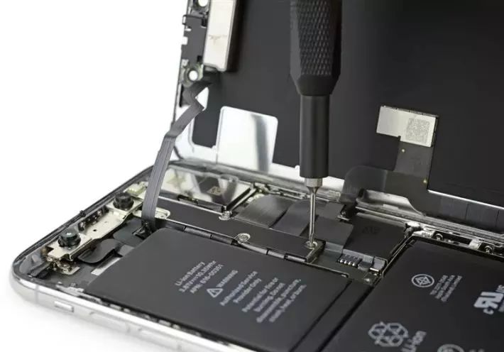
Now, let’s move on to the battery.
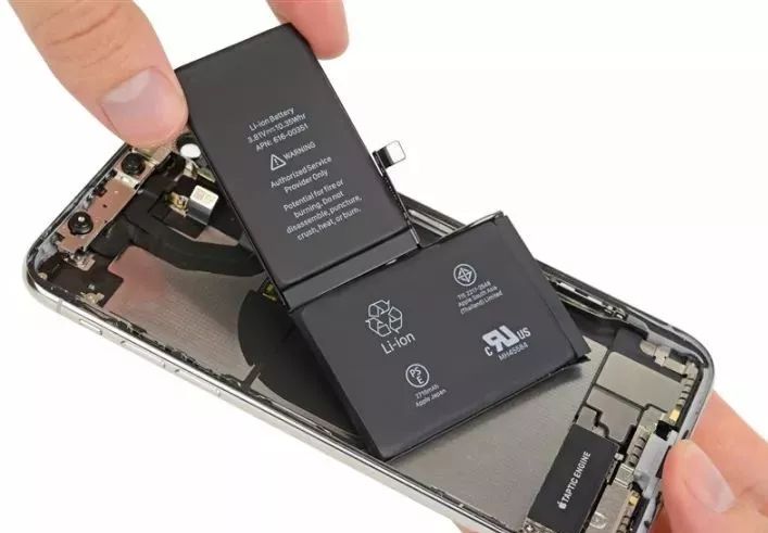
Although it's split into two parts, they are connected as one.
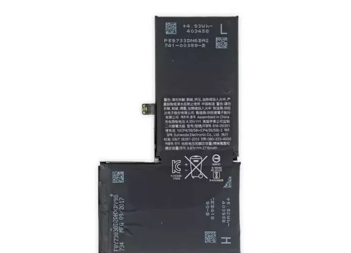
The battery specifications are 10.35W, 2716mAh, 3.81V, which is slightly higher than the iPhone 8 (10.28Wh) and even surpasses the Galaxy Note 8 (12.71Wh).
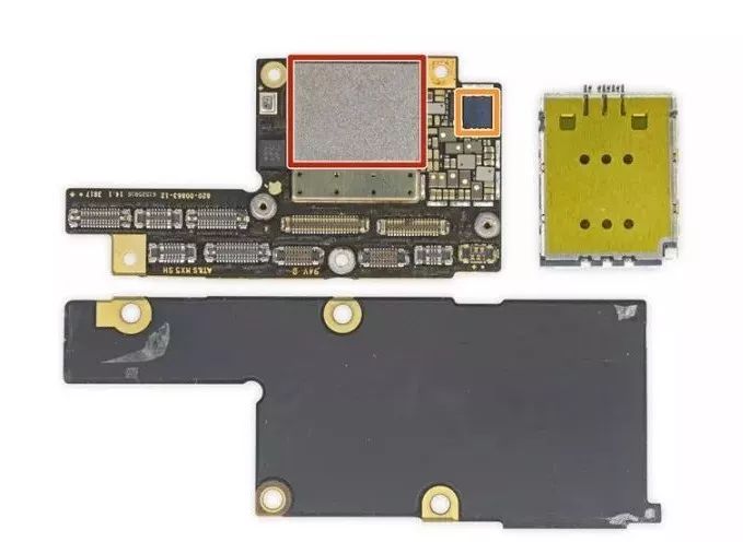
The TrueDepth camera system is definitely one of the key highlights of the iPhone X, as it powers the Face ID facial recognition feature.
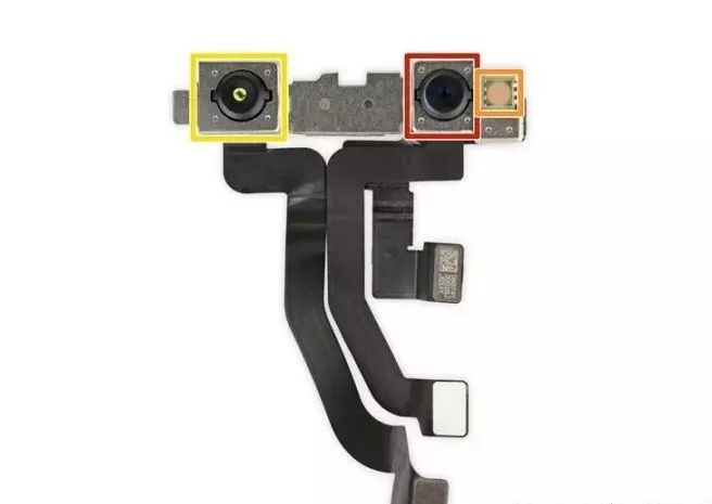
The red frame represents the front camera, the orange is the infrared dot matrix projector, and the yellow is the infrared camera.
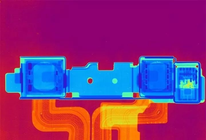
Here’s the X-ray view of the camera system.
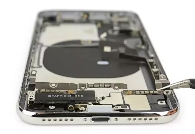
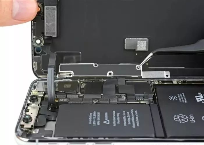
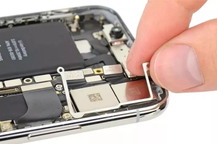
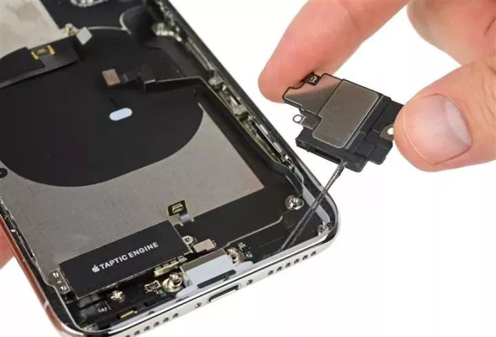
Now, removing the Taptic Engine.
The bottom speakers and waterproofing glue are also visible.
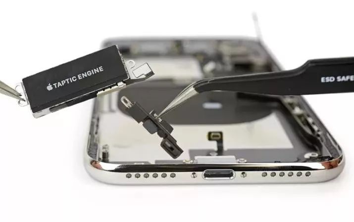
Waterproof parts and the "pseudo horn" are here.
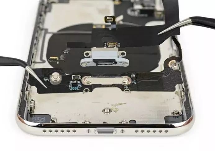
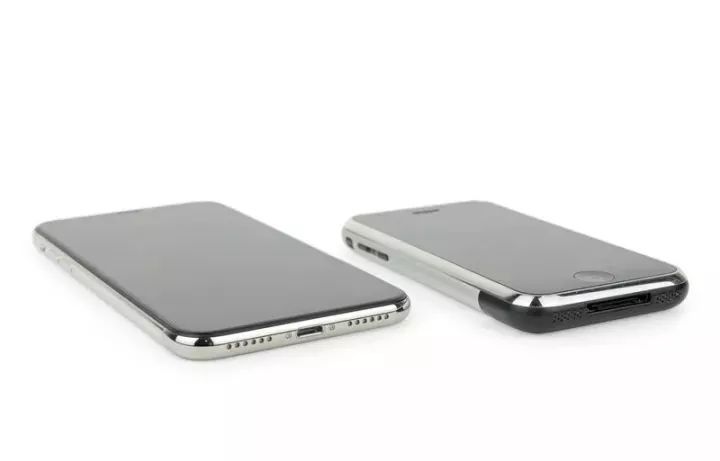
The Lightning interface is clearly visible.
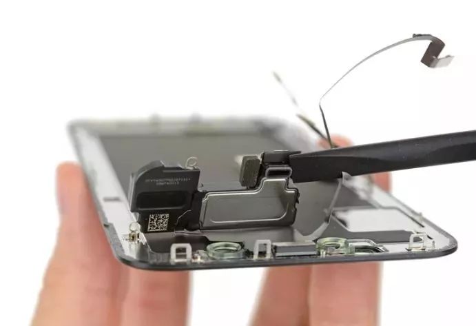
Going back to the front panel, the first component is the earpiece speaker, and its structure has been redesigned.
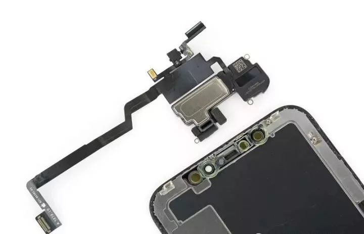
This is definitely the most complex front panel, housing speakers, microphones, ambient light sensors, floodlight sensing elements, and distance sensors.
After removing all components, the screen is finally taken out.
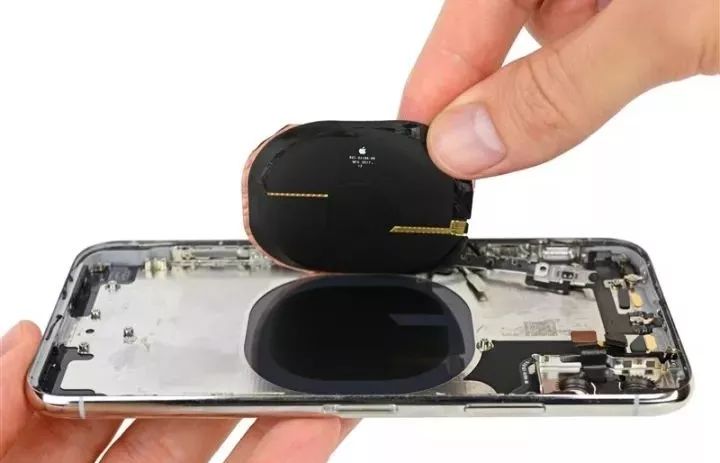
Now, it's time for the wireless charging circle.
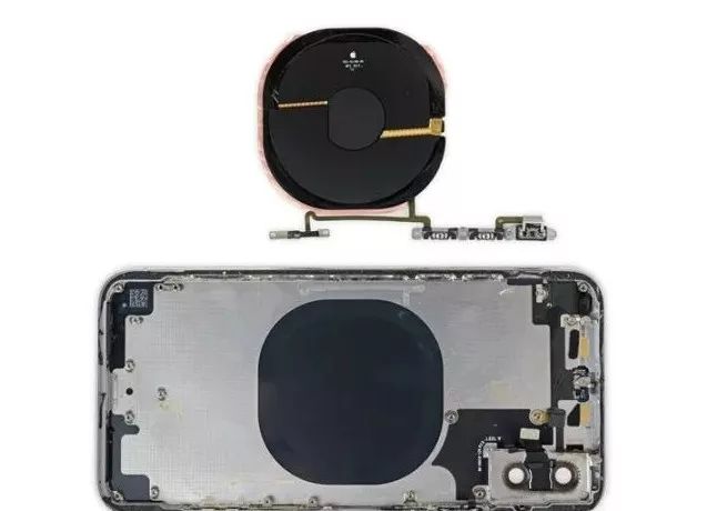
It connects to the volume button, mute switch, and an unknown sensor.
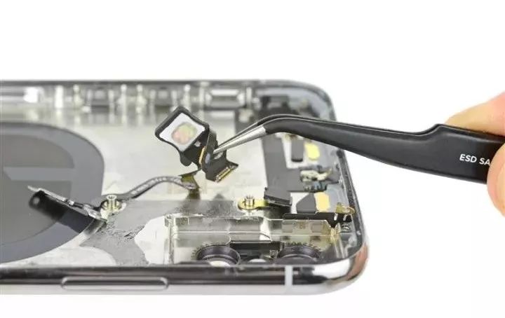
The flash and power button are located here.
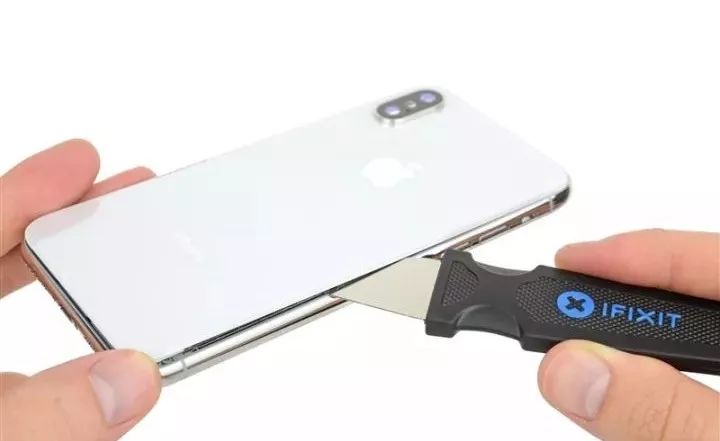
Back to the back of the phone, the glass backshell — the iPhone 8 Plus was accidentally broken during removal, so this time I'm being extra careful.
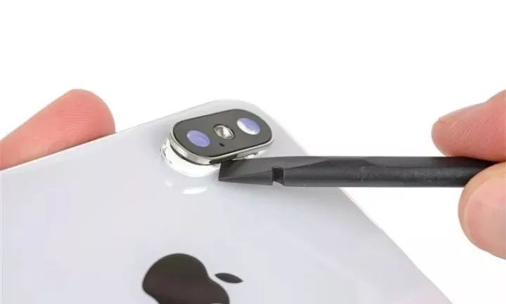
Also, the camera cover needs to be removed.
Smooth separation — no accidents this time.
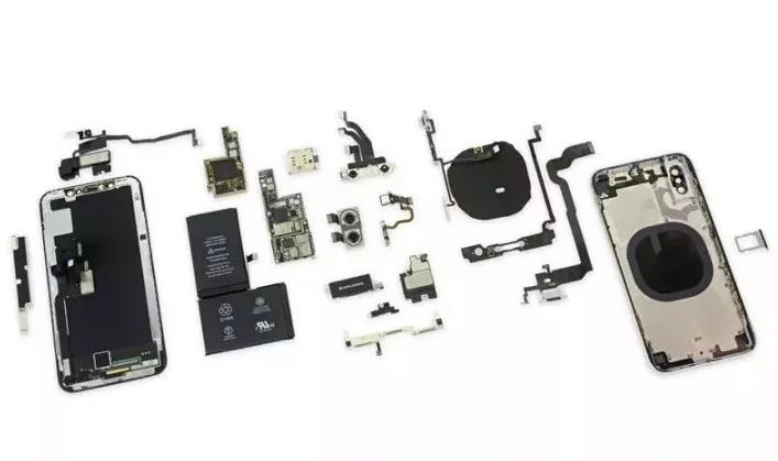
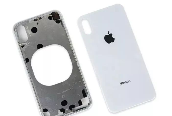
Finally, a full collection of all the parts.
UL XLPE Cable,UL3385 electronic wire,High-temperature resistant wires,Irradiation cross-linked wires
Jiangyin City Weicheng Special Cable Co.,Ltd , https://www.weichengcable.com