1. Test points should be added to the chip components that are not connected to any plug-in parts. The diameter of the test pads should range between 1.0mm and 1.5mm, making them suitable for online testing. The edge of the test pad must be at least 0.4mm away from the surrounding pad edges. The test pad should have a minimum diameter of 1mm and must be electrically connected. The center-to-center distance between two test pads should be no less than 2.54mm. If a via is used as a test point, an additional pad must be placed outside the via, with a diameter of more than 1mm.
2. Any hole that has electrical connections must be padded. All pads must have network properties, and if there is no component on a network, its name must be unique. The distance between the center of the positioning hole and the test pad center should exceed 3mm. For irregular shapes that include slots or pads, they should be uniformly placed on mechanical layer 1 (e.g., slotted holes like single insert or fuse).
3. For component foot pads with dense pitches (pin spacing less than 2.0mm), such as ICs or swing sockets, test points should be added if they are not connected to hand-pad pads. These test pads should have a diameter between 1.2mm and 1.5mm, ensuring ease of testing with an online tester.
4. If the pad pitch is less than 0.4mm, applying white oil can help reduce solder bridging during reflow.
5. Lead-in solder should be designed at both ends of the patch components in the dispensing process. The recommended width of the lead-in solder is 0.5mm, with a length typically ranging from 2mm to 3mm.
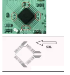
6. If a hand-welded component is present on a single panel, a tin bath should be created. The direction of the tin bath should be opposite to the direction of the solder flow, and the hole width should be between 0.3mm and 0.8mm, as shown in the example below:
7. The size and spacing of conductive rubber buttons must match the actual button dimensions. The PCB connected to these buttons should be designed as a gold finger, with a specified gold plating thickness (typically greater than 0.05μm to 0.015μm).
8. Pad size and spacing should align with the dimensions of the surface-mount components. This ensures proper soldering and avoids issues like poor solder joint formation.
a. When no special requirements are specified, the shape of the component hole, pad, and component foot must match. The pad should be symmetrically aligned with the center of the hole. For example, square component feet should match square holes and pads, while circular ones should match round ones. Adjacent pads should remain independent to avoid thin solder layers and solder pulling.
b. For adjacent component feet in the same row or compatible devices with different pin spacings, separate pad holes must be used. Especially for package-compatible relays, if PCB layout cannot accommodate separate pad holes, the perimeters of the two pads must be surrounded by solder mask to prevent solder shorting.
9. When designing multi-layer boards, pay attention to metal-shelled components. If a plug-in part is in contact with the board, the top layer of the pad should not be exposed. It should be covered with green oil or silk screen ink (e.g., the two-pin crystal or LED).
10. PCB design and layout should minimize slots and openings to maintain the structural integrity of the board and prevent weakening.
11. Valuable components should not be placed near the corners, edges, mounting holes, slots, or cutting areas of the PCB. These positions are high-stress zones and prone to cracking or solder joint failure due to mechanical stress.
12. Heavier components, such as transformers, should not be placed far from the positioning holes, as this may affect the board’s strength and cause deformation. During layout, place heavier components beneath the PCB (especially those that will go through wave soldering last).
13. Energy-radiating components like transformers and relays should be kept away from sensitive circuits such as amplifiers, microcontrollers, crystal oscillators, and reset circuits to avoid interference and ensure reliable operation.
14. For QFP packages using the wave soldering process, the IC should be placed at a 45-degree angle, and a solder pad should be added as shown in the image.
15. When over-wave soldering chip components, avoid opening heat-dissipating holes on the board or below the component body. This prevents solder from adhering to the upper board or component leads, which could cause foreign matter contamination during final assembly.
16. Large-area copper foil requires insulation tape to connect to the pad. To ensure good solder penetration, the pads on large-area copper foil should be connected to other pads via heat-insulating tape. Pads requiring more than 5A should not be designed as shown in the figure.
17. To prevent misalignment and tombstoning after reflow soldering of 0805 and similar chip components, the solder joints at both ends should be thermally symmetrical. The width of the connection between the pad and the printed conductor should not exceed 0.3mm (for asymmetric pads).
Low Speed and Middle Speed Generators with Low speed engine or middle speed engine
. Low speed diesel generators, 500rpm, 600rpm
. Middle speed diesel generators, 720rpm, 750rpm, 900rpm, 1000rpm, 1200rpm
. Voltage: 3kV, 3.3kV, 6kV, 6.3kV, 6.6kV, 10kV, 10.5kV, 11kV,13.8kV
. Frequency: 50Hz, 60Hz
Low Speed Generator,Middle Speed Generator,1000Rpm Diesel Generator,500Rpm Diesel Generator
Guangdong Superwatt Power Equipment Co., Ltd , https://www.swtgenset.com