In the first quarter of this year, Maxim developed a commercial TD-SCDMA mobile phone RF chipset, which made a battle for the commercialization of TD-SCDMA. Based on the reference design of this chipset, this paper discusses in detail some key technical issues that should be considered in the design of RF front-end of TD-SCDMA mobile phones.
This article refers to the address: http://
Compared with the other two third-generation mobile communication standards, TD-SCDMA has four technical features: two-way smart antenna technology, reverse link synchronization technology, reverse joint detection technology, and dynamic channel allocation technology, among which two-way smart antenna technology Benefit from its ability to send and receive the same frequency. In addition to the four technical characteristics, TD-SCDMA also has the advantages of low terminal cost and low operating cost. The terminal cost is low due to the TDD working mode; the operating cost is low due to the same frequency and frequency, and no pair frequency is needed.
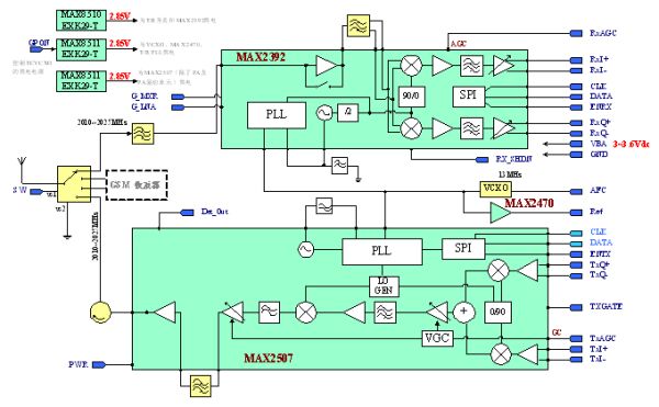
Figure 1: TD-SCDMA mobile phone RF unit reference design functional block diagram
Maxim's new commercial TD-SCDMA mobile phone RF chipset has two: MAX2507 and MAX2392. The MAX2507 is a transmitter chip that integrates all circuits from analog I/Q to amplifier output. The main functional blocks are: I/Q quadrature modulator, mixer, variable gain amplifier, power amplifier, RF local oscillator VCO, RF Phase-locked loop, IF local oscillator circuit, RF power detector. The MAX2392 is a zero-IF receiver chip that integrates all circuits from a low-noise amplifier to an analog I/Q output. The main functional blocks are: low-noise amplifier, I/Q quadrature demodulator, variable gain amplifier, and channel selection filter. , DC-Offset automatic removal circuit, I / Q amplitude automatic calibration circuit, VCO, phase-locked loop. For user-friendly design, MAXIM also offers a complete reference design (Figure 1) that has an effective RF PCB area of ​​6.6 square centimeters and operates at 3-3.6V and can be powered directly from a single-cell Li-Ion battery.
3GPP specifies a number of technical indicators for TD-SCDMA terminals. These indicators can be divided into three categories according to their purpose: one is to set the indicators to meet the needs of the system itself, such as transmitter output power level, power control accuracy , minimum controllable transmit power, transmit signal modulation accuracy EVM, receiver sensitivity, maximum receivable signal amplitude, frequency stability, etc.; second, indicators to reflect system robustness, such as receiver spurious response indicators , anti-monotone two-tone interference indicator, receiver adjacent channel selectivity indicator ACS, etc.; third, indicators to prevent the system from causing interference to the system itself or other systems, such as transceiver spurious emission indicators, transmitters Adjacent channel power leakage ACLR, transmission signal frequency domain template, transmitter intermodulation indicators, etc. For a detailed discussion of these indicators, please refer to the relevant 3GPP standards. This article takes the MAXIM reference design as an example and discusses only some of the challenging metrics.
ACLR indicator
The ACLR indicator is an indicator set to prevent the transmitter from interfering with adjacent frequency channels. It is also an important indicator for measuring the degree of nonlinear distortion of the transmitter. The TD-SCDMA signal is a non-constant envelope modulation. Its shaping filter is a root raised cosine filter with a roll-off factor of 0.22. Therefore, when there is nonlinear amplitude compression in the channel, new signals will be generated on both sides of the TD-SCDMA signal spectrum. The spectral component, the ACLR indicator refers to the ratio of the signal falling into the adjacent channel to the power of the primary channel signal. The TD-SCDMA standard stipulates that the adjacent channel ACLR indicator should be no more than -33dBc, and the indicator should be no more than -43dBc for each channel. However, when the signal power leaking to the adjacent channel is less than -55dBm, the ACLR indicator can be ignored. The MAXIM reference design has a large margin for the adjacent channel and the channel-by-channel ACLR indicator at the maximum transmit power.
Another feature of the MAX2507 is that it does not become very good at small signal transmission. It seems to be a disadvantage. In fact, this is precisely the originality of MAXIM engineers when designing the MAX2507. The MAX2507 guarantees that the ACLR indicator can meet the standard requirements at all transmit power levels, and has a certain margin while adaptively adjusting the power amplifier bias current according to the transmit power level, which makes the chip very power-saving in practical applications.
Transmitted signal spectrum template
The transmit signal spectrum template and the ACLR are both indicators for preventing the transmitter from causing interference to the adjacent frequency channel, and are also caused by the nonlinear amplitude compression of the channel. Compared with the ACLR index, the indicator is more strict. . The ACLR indicator only roughly specifies the ratio of the regenerated spectral component to the main channel spectral component power, while the spectral template specifies the relative magnitude of the regenerated spectral component in the range of 0.8 MHz to 4 MHz from the carrier. If you have tested some linear power amplifiers, you will find that sometimes the ACLR indicator is very good, but it does not meet the requirements of the spectrum template. The reason is that the reproduced spectral components are asymmetric with the upper and lower sides, and the shape of the sidebands is not imagined. The superposition shape of the 3rd and 5th order spectra is quite different from the ideal nonlinear product spectrum because it is related to the input and output matching of nonlinear devices. Although the MAX2507 has been designed with a 50 ohm input-output impedance for customer convenience, the circuit before and after the MAX2507 power amplifier is not always ideal, resulting in asymmetry in the regenerated spectral components and convex hull at some frequencies. Appears to meet the requirements of the spectrum template. To solve this problem, MAXIM designed a clever circuit inside the MAX2507 to compensate for the non-ideality of the external circuit by changing the register value, so that the problem can be easily solved.

Figure 2: Example of cross modulation
Transmit signal modulation accuracy EVM
EVM is an important indicator to measure the modulation accuracy of the transmitter's transmitted signal. It should be noted that this indicator is not simply to define the modulation accuracy of the RF signal. Instead, it first maps the RF signal to the I/Q plane, and then passes the matched filter and then samples. Obtain discrete I/Q values, and EVM measures the accuracy of the discrete I/Q values. It is not the same as the accuracy of the RF signal. The reason is that the shaping filter is used to find the discrete I/Q data points. In the frequency domain, the filter can suppress the out-of-band noise, thus improving the modulation accuracy. index. The 3GPP standard also states that the frequency and phase of the local oscillator during demodulation should be adjusted as much as possible, and all possible measures should be taken to minimize the final error. This means that some distortion and interference in the RF modulated signal will not occur. Counting EVM values, including linear distortion of the RF channel, carrier leakage, phase shift deviation of the I/Q quadrature modulator, and imbalance of the amplitude of the quadrature component and the in-phase component, so there are two other factors that affect the EVM index. Big factors: phase noise and nonlinear products. Equation 1 is a simplified formula used to estimate the EVM value.
EQ1
Among them, ACLR refers to the ACLR measurement value of the adjacent channel, Qrms is the cumulative phase error, and 9.5 is a correction value for the TD-SCDMA standard.
To verify that Equation 1 is correct, we first use the ESG signal source to generate a simple QPSK I/Q signal, where the chip rate is 1.28M, and the shaping filter is a root raised cosine filter with a 0.22 roll-off factor. At the input of the reference design shown in Figure 1, the reference design is adjusted to have an output power of 21dBm. At this time, the EVM is equal to 3.5% and the adjacent channel ACLR is -38.5dBc using FSIQ. Next we remove the ESG signal source. The TxI+ of the reference design is shorted to ground, so that a sine wave signal is obtained at the antenna port, the phase noise of the sine wave is measured by FSIQ, and the cumulative phase noise in the range of 1 kHz-1 MHz is calculated to be about 1.5 degrees. We substitute the above test results into Equation 1 to obtain:
EQ2
Comparing EVM measurements with calculated values, the error is less than one percentage point. It can be seen that Equation 1 is still very effective as an EVM estimation formula. The 3GPP standard requires that the EVM index be no more than 17.5%. From the above test results, it can be seen that the reference design shown in Figure 1 has a large margin.
Receiver sensitivity and NF
Receiver sensitivity is a system indicator. Not only the performance of the receiver RF channel affects this indicator, but also the demodulation algorithm of the baseband unit affects the indicator. It is obviously inappropriate to use this indicator to directly measure the performance of the RF receiver. The degradation of the small signal by the receiver RF channel is mainly the effect of additive white noise, which reflects the noise figure of the receiver. Phase noise also affects signal reception quality, but the effect of relative additive white noise on small signals is minimal, so the effect of phase noise is not considered here. Therefore, when the receiver baseband unit is determined, the receiver sensitivity signal level has a direct correspondence with the overall noise figure. The 3GPP TR 25.945 standard states that as long as the receiver noise figure is not greater than 9 dB, the whole machine should meet the sensitivity index (sensitivity level is -108 dBm). It also implies that if there is still a problem, it should be the problem of baseband demodulation. The RF receiver has nothing to do with it. The reference design shown in Figure 1 has a noise figure of approximately 5.7 dB, which is 3.3 dB margin relative to the minimum requirement of 9 dB. Therefore, the sensitivity of the mobile phone using the RF chipset should be -111 dBm.
Receiver nonlinearity requirements
Many of the many indicators of the 3GPP TD-SCDMA standard are related to receiver nonlinearity. These indicators are summarized into two categories: one is an indicator set to prevent performance degradation caused by strong interference in small signals, such as blocking and spurious response. Two-tone intermodulation; the other type refers to the signal itself is too strong, only one indicator here is the maximum input signal level indicator. In order to flexibly respond to these metrics and consider the power saving requirements of mobile phones, MAXIM has designed a variety of operating modes for the receiving chip MAX2392. The MAX2392's low-noise amplifiers have two high-low gain modes. The mixer also has two gain modes. The mixer also has two linearities. This combines the MAX2392 with four distinct modes: HGML, HGHL, and MG. LG. HGML refers to the high gain medium linearity mode where the low noise amplifier is in a high gain state and the mixer is in a high gain low linearity state. HGHL refers to the high gain and high linearity mode when the low noise amplifier is in a high gain state and the mixer is in a high gain and high linearity state. MG refers to the medium gain mode, where the low noise amplifier is in a high gain state and the mixer is in a low gain state, independent of the linearity of the mixer. LG refers to the low gain mode, where both the low noise amplifier and the mixer are in a low gain state, independent of the linearity of the mixer. The following is a detailed discussion of some specific non-linear indicator requirements.
a) Receiver maximum input signal level indicator. This indicator involves two problems with the receiver: the receiver channel gain control range, because this indicator specifies the maximum input signal level of the antenna port, and the sensitivity indicator specifies the minimum input signal level. We always want the level at the baseband interface. Constant, this requires that the channel gain control range is at least greater than the difference between the two specifications; another RF channel specification involved in this indicator is that the channel cannot be significantly limited at such a large signal level. . For this metric, MAXIM recommends setting the MAX2392 to a low gain mode. The reference design shown in Figure 1 measures an input 1dB compression point of -11.6dBm in the low gain mode, and the maximum input signal level is -25dBm, which is clearly satisfactory.
b) Spurious response and blocking indicators. The spurious response is mainly for the superheterodyne receiver. The spurious response point is also called the parasitic channel, which is the combined frequency of the RF local oscillator and the intermediate frequency. Compared to general blocking, when interference falls on these parasitic channels, it can cause greater harm to the system. The MAX2392 is a zero-IF receiver, so the problem is not obvious. The blocking indicator is further divided into a blocking indicator in the band and an out-of-band blocking indicator. The impact of the out-of-band blocking indicator on the system can be partially solved by the front-end RF filter. The influence of the blocking signal on the system has four aspects: the influence of reciprocal mixing, the influence of cross modulation, the influence of the components of the blocking signal, and the influence of the blocking signal directly on the input port of the baseband unit through the channel filter. The reciprocal mixing effect refers to the influence of the interference signal and the local noise sideband mixing product on the system. It is related to the local oscillator phase noise index and has nothing to do with the channel nonlinearity index, which will be discussed in detail later. The effect of blocking signals directly through the channel filter is related to the out-of-band rejection characteristics of the channel filter, and is independent of the channel nonlinearity. We also discuss this effect later.
Figure 2 is an example of an amplifier to illustrate the cross modulation phenomenon, and the mixer also has a cross modulation phenomenon. The signal at the f1 frequency point in Figure 2 can be considered as a blocking signal, assuming that its power spectral density function is a rectangular function, and the point frequency signal at frequency f2 is the desired signal. It is seen in the figure that there is a triangle at f2 in the output signal spectrum. The type spectrum appears, which is also called the cross-modulation product. The size of the cross-modulation product is related to the third-order cut-off point of the channel. When the input blocking signal is a stationary normal process, the power of the cross-modulation product can be calculated by Equation 3:
EQ3
Even if the desired signal at the frequency point f2 is not a point frequency signal, the cross modulation product still exists, and the level is also given by Equation 3, except that the spectral shape of the cross modulation product is no longer a triangle, but a triangle and signal power. Convolution of the spectral density function. The formula obtained above is based on the assumption of normal noise. The general interference signal is closer to the constant envelope signal than the normal noise, and the cross modulation product is smaller. When the interference signal is a constant envelope, the cross modulation product Zero.
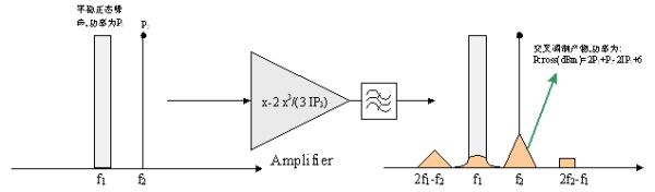
Figure 3: Model of the influence of the secondary component of the blocking signal on the system
The 3GPP stipulates that when there is a modulation type of interference signal at 4.8 MHz, the level is -49 dBm, and the system sensitivity can be reduced by 3 dB. If we believe that the decrease in sensitivity is due to the cross-modulation product, the indicator has no problem as long as the cross-modulation product power is not greater than the in-band total noise power at the sensitivity level. Assuming that the noise figure of the receiving channel is 9dB, which is the minimum required by the standard, the equivalent third-order cut-off point required by the index can be derived. The third-order cut-off point is related to the frequency offset of the input blocking signal, because the receiving channel includes Channel selection filter.
EQ4
The model of the influence of the secondary component of the blocking signal on the system is shown in Fig. 3. The secondary distortion product of the blocking signal consists of three parts. When the blocking signal is a stationary normal process, the three parts of the product are equal in power, and the power level is shown in Figure 3. Note that the formula in Figure 3 is based on the assumption of normal noise. The general interference signal is closer to the constant envelope signal than the normal noise, and the low-frequency AC product will be smaller. When the interference signal is a constant envelope, the low-frequency AC The product is zero. The interference model is only for a zero-IF receiver. The zero-IF receiver can be simply equivalent to a mixer. The mixer output contains various combinations of the local oscillator frequency and the input signal frequency, and the interference model is It is the combined component of the secondary of the input signal and the local frequency of the local oscillator. The low-frequency AC component and the DC component of the combined component fall within the frequency band we want, which will affect the system performance. The effect of the DC component is also known as the DC-offset. The MAX2392 has a dedicated DC-Offset removal circuit, while the low-frequency AC component cannot be removed.
The 3GPP stipulates that when there is a modulation type of interference signal at 4.8 MHz, the level is -49 dBm, and the system sensitivity can be reduced by 3 dB. If the decrease in sensitivity is caused by the low-frequency AC product in the quadratic component of the blocking signal, the indicator has no problem as long as the product is not greater than the total in-band noise power at the sensitivity level. Assuming that the receiving channel noise figure is the minimum required by the standard, 9 dB, the equivalent second-order cut-off point required by the index can be derived. The second-order cut-off point is related to the frequency offset of the input blocking signal because of the receiving channel. Includes channel selection filter.
EQ5
The MAX2392 has four modes of operation. When there is no interference and the signal is weak, the HGML mode is recommended. The above blocking indicator should be a weak signal and strong interference. It is recommended to set the MAX2392 to HGHL mode. Through discussion we get two RF channel indicators: IP 2 and IP 3. For IP 3 , the two-tone intermodulation indicators discussed below will have higher requirements. Equation 5 gives that the IP 2 required for the blocking index should be greater than 3 dBm. The reference design of Figure 1 has a large margin on this indicator.
c) Two-tone intermodulation indicators. Both the zero-IF receiver and the super-heterodyne receiver will face the problem of two-tone intermodulation interference. The main factors affecting this index are the mixer and the active devices in the previous stages. The circuit behind the mixer has little effect on this index due to the channel filter. 3GPP stipulates that there are two interfering signals in the TD-SCDMA terminal, one is the modulation type interference signal, the level is -46dBm at ±6.4MHz, and the other is the point frequency type interference signal, at ±3.2MHz, the level At -46dBm, the system sensitivity can be reduced by 3dB. If the decrease in sensitivity is considered to be caused by the intermodulation product, the indicator has no problem as long as the power of the product is not greater than the total in-band noise power at the sensitivity level. Assuming that the receiving channel noise figure is 9 dB required by the standard, the equivalent third-order cut-off point required by the index can be derived. The third-order cut-off point is related to the frequency offset of the input interference signal because the receiving channel Includes channel selection filter.
EQ6
For the discussion of intermodulation suppression indicators, the MAX2392 should be set to HGHL mode, in which the reference design shown in Figure 1 can fully meet the requirements of this specification with a certain margin.
Receiver channel selectivity requirements
The indicators related to the receiver's linear amplitude-frequency characteristics specified by the TD-SCDMA standard include: ACS, blocking, spurious response, and intermodulation suppression. When the blocking and spurious response points are far away from the TD-SCDMA band, they can be solved by selecting the band filter of the RF front end. For the blocking interference and spurious response points in the band, and the two-tone intermodulation interference, it is necessary to pass the channel filter. Filter out. For receivers with superheterodyne structure, the channel filter is the surface acoustic wave filter usually used after the mixer. The MAX2392 is a zero-IF receiver chip whose channel filter is an active low-pass filter on the I/Q branch, which is integrated inside the chip and has high specifications. The ACS is the only pure radio frequency specification specified by the 3GPP for the receiver. It directly stipulates that the receiver channel filter suppresses the adjacent channel (±1.6MHz) by 33dB. The in-band blocking specification specifies that when there is -61dBm modulation interference at ±3.2MHz, or -49dBm modulation interference at ±4.8MHz, the system sensitivity is allowed to drop by 3dB. If the sensitivity is considered to be due to blocking interference directly applied to the input port of the baseband unit through the filter, regardless of the effects of nonlinearity and reciprocal mixing, as long as the transmitted interference power is not greater than the sensitivity level. The total noise power, then there is no problem with this indicator. Assuming the receiver channel noise figure is the minimum required by the standard (9dB), the out-of-band rejection characteristics of the channel filter required by this indicator can be derived:
EQ7 EQ8
The two interfering signals specified by the two-tone intermodulation index are one point frequency interference, the other is the self-adjusting type interference, the point frequency interference has obvious characteristics, and the baseband is easy to deal with. Only the influence of the modulated interference is considered here. The same analysis method with the inner block is available:
EQ9
At this point, we have four parameters for the out-of-band rejection of the channel filter, that is, the relative suppression of the ±1.6MHz channel should be no less than 33dB, and the relative suppression of the ±3.2MHz channel should be no less than 43dB, to ±4.8MHz channel. The relative suppression should be no less than 55dB, and the relative suppression of ±6.4MHz channel should be no less than 58dB. The MAX2392 channel selection filter specification is much higher than the above four requirements. Refer to the MAX2329 data sheet for the filter's frequency response characteristics.
Phase noise
The TD-SCDMA standard does not explicitly propose the transceiver phase noise index, but many other indicators specified by the standard are related to the phase noise: the EVM index of the transmit signal modulation accuracy is related to the phase noise of the phase-locked loop of the transmitting channel, and Equation 1 gives them The relationship between EVM is mainly determined by nonlinear indicators, unless the phase-locked loop index is too poor; the receiver sensitivity is related to the receiver channel local oscillator phase noise index, but the sensitivity index does not require high phase noise, even 16QAM. The signal is also the same, the main effect of sensitivity is additive white noise; the frequency stability index is related to the receiving and receiving phase-locked loop indicators. The frequency stability index seems to be talking about the frequency accuracy problem, but carefully pondering the test methods specified by the standard, we will understand that the frequency stability index is related to the noise figure, the local oscillator phase noise of the receiving channel, and the baseband unit frequency estimation algorithm. . The indicator mainly depends on the baseband algorithm and the phase noise of the phase-locked loop of the transmitting channel. The phase-locked loop of the transmitting chip MAX2507 in the reference design shown in Figure 1 is a ∑-Δ phase-locked loop with a very high phase noise index; blocking index, two-tone The intermodulation indicator is related to the receiver channel local oscillator phase noise indicator. One way for the blocking indicator and the two-tone intermodulation indicator to affect the system is to rectify the mixing. Both the blocking suppression index and the two-tone intermodulation index are mentioned to allow the receiver sensitivity to drop by 3 dB. If the reason for the decrease in sensitivity is all caused by the reciprocal mixing product, as long as the product power is not greater than the sensitivity level The total internal noise power, there is no problem with this indicator. It is still assumed that the receiver channel noise figure is the minimum required by the standard (9dB), and an indicator that limits the noise floor of the local oscillator can be derived:
EQ10
The maximum interference power mentioned in the blocking and dual tone intermodulation index is -46dBm point frequency signal, which is 3.2MHz away from the center of the useful signal. Substituting this value into the above equation, an index about the local oscillator phase noise of the receiver is obtained: The phase noise must be better than -119dBc/Hz outside the center of 3.2MHz. The phase noise at this point of the MAX2392 is far superior to this minimum requirement.
Zero IF receiver and DC-Offset
However, the zero-IFset receiver has DC-offset problem, and the DC-offset is generated for several reasons: the local oscillator self-mixing, the mixer nonlinear term distortion product, and the balanced mixer forward and reverse conduction time are not equal. Balance the mixer load imbalance. Regardless of how it is generated, the focus is on removing this DC offset. For a circuit, it removes the DC component and retains the AC component. It must be a high-pass filter. How should the high-pass filter be designed and how can the filter parameters be easily adjusted? There are generally three cases: one is to use a fixed high-pass filter, so that it is constant, the advantage is simple, the shortcoming is long response time; the second is to use a high-input high-pass filter, the filter is only at a certain time Function, fast response, the circuit remembers its response final value after the response, and then uses the final value to cancel the DC offset on the channel. The disadvantage is that after the environment changes, the recorded previous response final value cannot be cancelled. The DC offset; the third is to flexibly change the inflection point of the high-pass filter, which obviously combines the advantages of the above two methods.
The Ability To Connect An Ethernet Device Via A USB Port Is Called Ethernet Via USB. There Are Many Low-Cost Commercial Adapters That Can Do This And Are Usually Implemented As A Bridge Between The Real Ethernet And Ethernet Networks In The USB, As The Degree Of Integration Continues To Increase, The Number Of Chips On The Network Card Continue To Reduce, Although The Manufacturers Now Produce A Wide Range Of Network Cards, But Its Function Is Similar.
1, USB Network Adapter Interface Type Is Divided Into Three, USB 2.0 / USB 3.0 / Type-C, The Card Transfer Rate Is Divided Into 10Mbps / 100Mbps / 1000Mbps Network Transmission, Experience Fast Steps! Simple And Stylish, Easy To Carry, No WIFI Like To Enjoy The Same Network, Efficient And Stable, Multi-System Free Drive, Better Use USB Card, Apple OS System / Windows System,
2, USB Network Adapter Supports Plug And Play, A Single Windows System Can Not Automatically Drive, Just Download The Driver Wizard Or Drive Life Cycle, Software, Automatic Detection And Installation Of The Drive Available.
3, USB Network Adapter Support Sleep And Remote Wake-Up Function,
4, USB Network Adapter Supports Two VLAN ID Filtering.
5, USB Network Adapter Support Automatic MDIX, Whether It Is Cross-Network Cable Or Through The Network Cable Can Automatically Identify!
6, Support Full / Half Duplex Fast Ethernet Connection, Support IPV4 / IPV6 Network
USB Gigabit Ethernet Adapter

USB 3.0 Network Adapter
USB Network Adapter
USB 3.0 Network Adapter, USB 3.0 Gigabit Ethernet Adapter, USB 2.0 Ethernet Adapter mac, USB 3.0 Ethernet adapter Driver , Type-C3.1 Network Adapter
Shenzhen JunYuanJie Electronic Technology Co., Ltd. , http://www.usb3c.com