Low Noise Amplifiers (LNAs) play a crucial role in various high-sensitivity applications such as radio astronomy, satellite communication, and radar systems. Their primary function is to amplify weak incoming signals while minimizing noise, thereby ensuring the integrity of the received information. A key performance metric for LNAs is the Noise Figure (NF), which directly impacts the system's overall sensitivity. Therefore, the design of an LNA is critical in determining the performance of the entire receiver system.
In this paper, we focus on the design of a low-noise amplifier for a GPS receiver. The main specifications of the designed LNA include an operating frequency range of 1.52 GHz to 1.60 GHz, a noise figure of less than 1.6 dB, an input voltage standing wave ratio (VSWR) of less than 2, and an output VSWR of less than 1.5.
1.1 Device Selection
Selecting the right transistor is essential for achieving low noise and high gain. We chose the PHEMT GaAsFET transistor ATF-54143 from Agilent, known for its excellent noise performance in the desired frequency range. Before proceeding with the design, we created a small-signal model of the transistor. To ensure accurate simulation, we used the models provided by Murata for inductors and capacitors. Specifically, we selected the chip inductor LQWl8 and the chip capacitor GRMl8, both of which offer high Q values, particularly at 1.6 GHz, where the inductor has a typical Q value of 80.
1.2 DC Bias Design
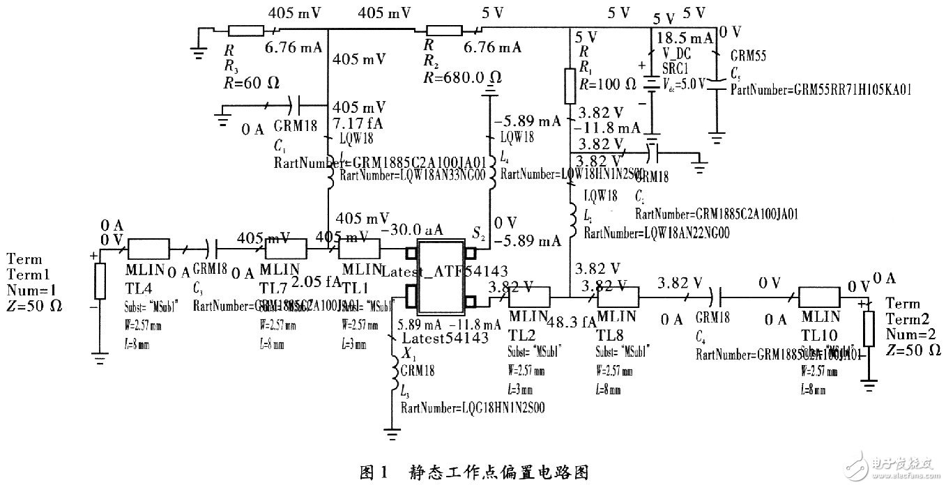
Setting up the correct DC bias is crucial for achieving optimal performance. The static operating point affects the noise, gain, and linearity of the amplifier. For this design, a resistor-based passive bias network was chosen due to its simplicity and cost-effectiveness. The bias point was set to Vds = 3.8 V and Ids = 11 mA, based on the manufacturer’s datasheet. The resistors R1 = 60 Ω, R2 = 680 Ω, and R3 = 100 Ω were used to establish the operating point, as shown in Figure 1.
1.3 Stability Design
Ensuring the stability of the amplifier is vital for reliable operation. Two common methods are used to determine if a device is unconditionally stable: the first involves analyzing the stability factors, while the second uses the μ parameter defined as:
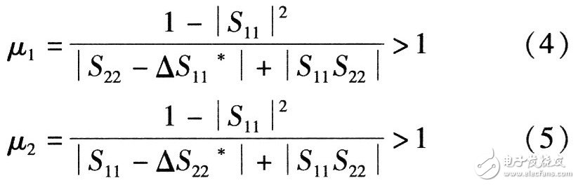
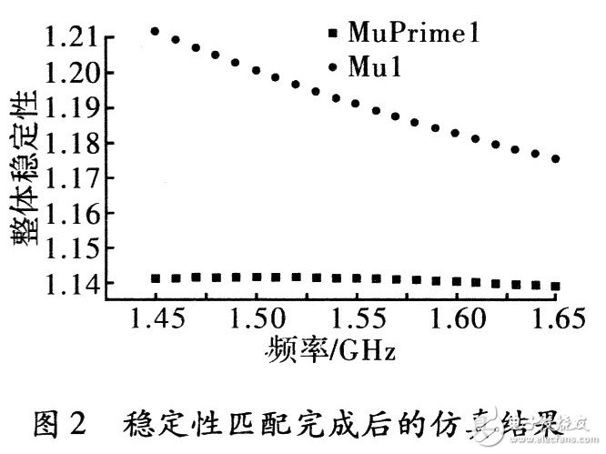
To enhance stability, two approaches can be used: adding a resistive load at the drain or introducing source inductive feedback. In this design, we opted for the latter, using an inductor between the source and ground to improve stability without significantly reducing gain. The simulation results, shown in Figures 2 and 3, confirm that the circuit remains stable across the entire operating band of 1.52–1.60 GHz.

1.4 Input and Output Matching Network Design
For the input matching network, we used a noise-optimal matching approach rather than conjugate matching. The input network consists of C4 and L5, which help reduce return loss and improve gain and stability within the band. L1 serves as a DC block and AC short, while C1 acts as an RF bypass. High-Q inductors are essential for minimizing noise at the input. The output matching network uses conjugate matching, consisting of C6 and L7, to further reduce return loss and increase gain. C2 acts as an RF bypass, and C5 decouples the power supply.
The component values were initially calculated using Smith software and then optimized using ADS. During optimization, it's important to carefully adjust sensitive parameters, define clear optimization goals, and avoid self-oscillation. This process ensures that the final design meets all required specifications.
1.5 Overall Circuit Optimization
After completing the DC bias, stability, and matching network designs, the basic structure of the LNA was established. However, further optimization was necessary to meet all performance requirements. Factors such as microstrip line width, grounding, and vias were considered during the overall simulation. The microstrip line was designed with a characteristic impedance of 50 Ω, and its width was calculated using Agilent’s Appcad software to be 2.57 mm for a substrate with a dielectric constant of 2.65 and a thickness of 1 mm.
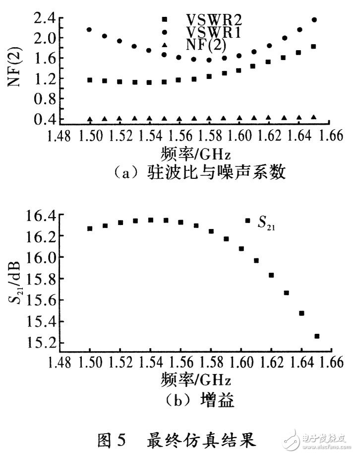
During the optimization phase, it's crucial to use tuning functions effectively. Starting with approximate parameter values and gradually refining them helps achieve the desired performance. The final simulation results, shown in Figure 5, demonstrate that the LNA meets all the design specifications, including low noise, good gain, and stable operation across the target frequency range.
110KV-220kv Oil Immersed Transformer
110Kv-220Kv Oil Immersed Transformer,Anti - Interference 110Kv Transformer,Low Loss 110Kv Oil-Immersed Transformer,High Load Capacity 110Kv Oil-Immersed Transformer
Tianhong Electric Power Technology Co., Ltd , https://www.tianhongtransformer.com