Signal integrity is a critical system engineering discipline that focuses on analyzing and mitigating the negative effects of noise, distortion, and signal loss in high-speed digital communication systems. It plays a vital role in ensuring the performance and reliability of high-speed links at the system level. However, maintaining electrical performance integrity remains a significant challenge in the "Siege Lion" of high-speed circuit design. Experienced engineers, often referred to as "old birds," are adept at applying signal integrity principles and utilizing simulation and testing tools effectively to quickly resolve various circuit issues.
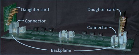
Today, we’ll dive into the tools used in signal integrity analysis and provide hands-on video tutorials to help you elevate your technical skills. In high-speed digital signal transmission, a channel refers to the complete electronic path from the transmitter's IO buffer to the receiver’s IO buffer. This path may include components such as chip packages, PCB traces, connectors, and cables. A simple channel could be a straightforward routing from the transmitter to the receiver, while a complex one, like a backplane, consists of multiple elements as shown in Figure 1.
When modeling a channel, it’s essential to focus on three key characteristics: impedance, loss, and delay or phase. Impedance is influenced by the mechanical structure, dielectric constant, and metal conductivity. Mismatches in impedance can lead to signal reflections, causing ringing, overshoot, and undershoot. Channel loss is also crucial for SERDES design, with dielectric and conductor losses typically being frequency-dependent. This limits the bandwidth and maximum bit rate a channel can support. For DDR systems, precise control of the phase difference between command, address, clock, DQ, and DQS signals is essential.
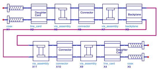
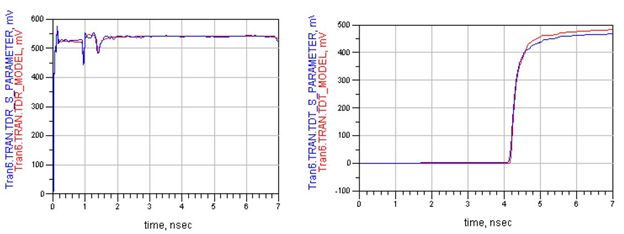
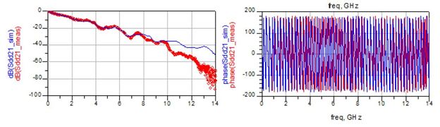
Channel components can be modeled using formula-based transmission line models, electromagnetic simulations, or measurement-based approaches. The accuracy of each model depends heavily on the precision of material parameters. Once individual components are accurately modeled, they can be cascaded to form a complete channel model (as shown in Figure 2). Impedance and delay can be estimated through TDR simulations (Figure 3), while insertion loss and phase can be evaluated via S-parameter simulations (Figure 4).
Now that you have a basic understanding of high-speed channel modeling, let’s move on to how to build one. The video below will guide you through creating a high-speed channel model with specific frequency loss characteristics.
(Want to learn more about ADS for signal integrity and power integrity analysis? More details will follow.)
After reading this, do you feel confident about using ADS to build a high-speed channel model? With proper modeling, you can adjust link parameters freely, observe their impact on the model’s behavior, and ultimately identify the optimal solution. Once the simulation and optimization are complete, it’s time to apply the results to the actual circuit and perform necessary debugging based on real-world conditions to ensure the final product meets expectations.
At this stage, Keysight’s oscilloscope becomes an essential test tool, enabling accurate and efficient testing of various signal characteristics, which significantly speeds up the verification process.
Of course, experienced engineers often go further—they aim to predict the outcome before the new board is even manufactured. This helps improve optimization efficiency, reduce costs, and shorten the product development cycle. Keysight’s oscilloscope offers another powerful tool: the N8900A offline software.
By importing S-parameters obtained from ADS simulations into the N8900A, you can embed and de-embed the measured eye diagram of the high-speed link’s front end. This allows for a more accurate evaluation of the channel model’s performance under real-world conditions, helping you find valuable debugging insights and directions.
166mm Mono Solar Panel
In terms of production capacity supply, although the current photovoltaic market is battling around the size of 182mm and 210mm, it has its own advantages to occupy a certain proportion of the market share.
PERC 166mm Solar Cell
with Solar Panel`s efficiency up to 21.2%
Sunket 166mm solar panel use 166mm 9BB solar cell, increases the wafer size, optimizes the layout profoundly and decreases the invalid power generation area.
1.Half Cell Technology
The half-cut cell design can decrease the power loss by the shadow effectively. The optimized circuit design not only realizes the maximum power output but also assures the reliability of solar panels.
2.MBB Technology
Sunket 166mm Solar Panel adopts 9 busbar technology. More busbars of the cell decrease the current transverse propagation path by 50%, effectively reduce the internal loss, and improve power of solar panels.
Standard & All Black Solar Panels
max power breaks through 460W+
01. 120/144Cells Solar Panels
02. All Black Solar Panel for home use
03. 360W-460W+ Solar Panel, Suitable for residential roofs
Solar Panel,Solar PV Module,166 PV Module,166mm Solar Panel,166 Solar Panel
Wuxi Sunket New Energy Technology Co.,Ltd , https://www.sunketsolar.com