Keywords: Video A / D conversion, SAA7111A, AL251
1 Introduction?
Video signals include not only image signals, but also line synchronization, line blanking, field synchronization, field blanking and other signals. Many people often feel helpless about how to display analog video signals on various interface displays. The traditional scheme uses a lot of analog separation components, which is not only complicated but also difficult to debug. The scheme introduced in this article mainly adopts integrated circuit design, small size, low cost, few peripheral analog devices, all control can be implemented by software, initialization and waiting time is extremely short, can be suitable for digital multimedia applications such as board cards or small handheld terminals The system block diagram is shown in Figure 1. The system mainly includes two parts: one is the video decoding module, the purpose is to A / D convert analog video signals such as composite video and YC components, extract the synchronization and clock signals, and all the conversion circuits are concentrated in one chip; It is a video conversion module. Its function is to directly output analog RGB, digital RGB, or digital YUV video signals to realize the conversion from interlaced to progressive scanning. Since ordinary CVBS signals are interlaced, this part is necessary for progressive displays. The signal after it can be directly displayed or used in the video acquisition system, and can also be used in other formats (need to be converted). In addition, the FPD link (Flat Panel Display Link) transmission part can realize long-distance (up to 10m) digital RGB video display (digital RGB video signal frequency is too high to achieve long-distance transmission).

2 Decoder selection TV decoder can choose SAA7110 / 7111A / 7112/7113/7114/7115/7118 of PHILIPS company, KS0127 (S5D0127X01) of SAMSUNG company or VPC3211B of ITT company, they can be controlled through IIC bus interface, automatic identification Input analog video signal format, then decode and output 24bit / 16bit RGB or YUV digital signal and Hsync, Vsync, HAV (HREF) control signal and sampling clock. The decoded signal can be directly sent to the video conversion module or video acquisition system. According to the technical documents released by AVERLogic, PHILIPS 'decoder has the best decoding effect, followed by VPC3211B. Although KS0127 is powerful and cheap, the decoding effect is slightly inferior, and the biggest disadvantage of the chip is that the power consumption is too large (nearly 1W ). According to the author's research, SAA7114 has the best effect, but due to various factors, this solution uses SAA7111A, which uses CMOS technology, low power consumption (less than 0.5W), low voltage (3.3V), small size (1cm2), wide temperature range (? 10 ℃ -80 ℃), with the following characteristics:
(1) Automatically detect the field frequency of 50 / 60Hz, support the automatic conversion of NTSC and PAL system, and the brightness and color of NTSC? M / N / 4.43 / JAPAN, PAL? M / N / BGHI /, SECAM format video signals Degrees to process. ?
(2) Has 4 analog inputs: 4 composite video (CVBS) or 2 YC or 1 YC and 2 CVBS. ?
(3) CVBS or YC channels can be set to static gain control or automatic gain control (AGC). ?
(4) It has 2 channel comb filters for brightness and chroma, which can control the brightness, contrast, aperture and saturation. ?
(5) Line (HREF), field (VREF) synchronization, parity frame (RES1) and pixel clock (LLC) signals can all be derived from the pins. ?
(6) The following output formats can be supported: 4: 2: 2 (16-bit), 4: 2: 2 (CCIR601 8-bit), 4: 1: 1 (12-bit) YUV format or 8: 8: 8 (24-bit ), 5: 6: 5 (16-bit) RGB format.
(7) Boundary scan test circuit conforming to IEEE1149.1 standard scan logic. ?
(8) 64-pin LQFP package (size: 10mm × 10mm × 1.4mm), power consumption is less than 0.5W.
Since the chip has been introduced in many magazines, it will not be repeated here. ?
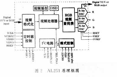
3 Video converter AL251 is a powerful display conversion control chip produced by AVERLogic, mainly used in LCD VGA display or video editing applications, it can receive interlaced NTSC or PAL, ITU? RBT601 (CCIR601) or square pixels, YUV422 or RGB565 digital signals are converted into analog RGB format video signals that ordinary PC monitors can receive and progressive digital video signals in YUV422 or RGB565 format for display on VGA LCD. AL251 has a variety of control functions, such as automatic identification of PAL system / NTSC, adjustment of screen position, filtering of video noise, OSD (on-screen display), video LUT (Lookup Table), POWERDOWN and other functions through the IIC interface of the microprocessor. Hard initialization can be performed without software control. AL251 has AVERLogic's unique digital signal processing technology, the processed image is smoother, with less flicker and jagged edges. The chip's power supply voltage is 3.3V or 5V, and it is packaged in an 80-pin QFP package.
The functional block diagram of AL251 is shown in Figure 2. ?
3.1 Input and output data format?
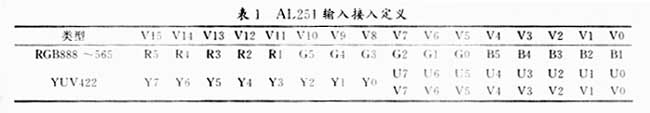
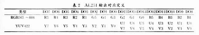
AL251 can input and output two data formats: YUV422 or RGB565. The input video format is determined by the pin INTYPE (1 is YUV422, 0 is RGB565), the input interface is shown in Table 1; the output video format is selected by the control register 08h, and the output interface is shown in Table 2. The accuracy of AL251 depends on the previous video decoder and does not require software control. It supports up to 1024 × 768. The VCLK is provided by the decoder. ?
3.2 On-screen display AL251 provides two channels to support the on-screen display (OSD) function to superimpose the control menu, text or title on the original output, and produce some special effects such as transparency, opacity, film, background, grid and so on. The internal channel implements a built-in OSD bitmap, and the external channel controls two stacked pins (OVLCTRL1 and OVLCTRL0) for displaying stacks on the screen and generating some special effects. Regardless of whether it is an internal channel or an external channel, OSD can only be used for analog video and output in RGB565 mode, not supported in YUV422 mode.
3.3 Border / Border color?
During analog output, AL251 can display all the pixels in the video signal source, so that it can display a larger area than the ordinary display. This is advantageous for DVD digital video sources, but for some VCR-like video sources, it will There are consequences of uneven borders. For this reason, AL251 controls the border by cropping the video source. In addition, the border color (24 bits) after cropping can be set through the register.
3.4 Register description?
AL251 has a total of 42 internal control registers. Among them, 00h ~ 04h is the configuration status register, used to display the company ID (46h), version number and chip serial number, and set the chip's working status (video signal input type and format); 08h, 09h are synchronization control and status register , Used to set the method and polarity of various synchronization signals, and report the current status of various synchronization signals; 0Ch ~ 0Eh is the boundary color register, which is used to set the red, green, and blue component values ​​of the boundary color; 10h ~ 13h is LUTOSD Register; 14h ~ 1Dh is a stack control register, used to set the stacking effect and color.
4 Link introduction In order to increase the transmission distance, FPD link connection can be used between LCD and AL251. This solution uses NaTIonal Semiconductor's LVDS (Low Voltage DifferenTIal Signaling) DS90C363 / DS90CF364 transmission kit, with a transmission distance of up to 10m. The chip is an 18-bit FPD link, operating voltage 3.3V, 48-pin TSSOP package, where DS90C363 is a transmitter, can be 18-bit RGB data and 3-bit LCD timing and control data (FPLINE / GHS, FPFRAME / GVS, DRDY / ENAB / GHREF) is converted into 3 groups of LVDS in one clock cycle. At 65MHz transmission clock frequency, the transmission rate of each LVDS channel is up to 455Mbps, and the data throughput is 170 megabytes per second. It is triggered by rising or falling edge; DS90CF364 is a receiver, which can convert the received LVDS data stream into TTL / CMOS data for high-speed long-distance transmission of multiple digital signals. The kit supports VGA, SVGA, XGA or higher resolution. In use, the designer does not need to change the original circuit connection relationship.
5 System hardware connection?
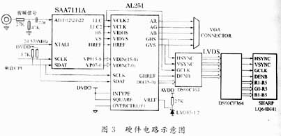
Figure 3 is a schematic diagram of the hardware circuit of the conversion system, using a 3.3V power supply. This system uses Cygnal's C8051F020 processor to control, select SHARP's LQ64D341 TFT LCD screen, resolution is 640 × 480, the interface is 18-bit digital RGB mode, the inverter uses TDK's CXA? M10A.
In the picture, the video signals of PAL / NTSC / SECAM can be input through the AI11 / AI12 / AI21 / AI22 channel of SAA7111A. If it is S terminal, it takes up two input channels. Among them, AI12 is connected to pin 3 of S terminal and AI22 is connected to S terminal. 4 pins, pin 1 and pin 2 of S terminal are grounded, the actual port can be set by software selection. The 24.576MHz reference clock signal is input through XTALI; AL251's VCLK, VIDHS, VIDVS, HREF are the line and field synchronization and sampling clock of the input video signal; SQUARE is the square pixel and CCIR601 selection setting (1/0), and CCIR mode is selected here; OVLCTRL0 / 1 is cascade control, 00 is no cascade; GHS, GVS are line and field synchronization for outputting video signals, and the analog / digital RGB interface shares these two pins; the LLC clock signal output by SAA7111A is directly connected to the GCLK pin of the LCD screen Connected, GHREF is the display enable of the LCD screen, VREF is used to simulate the RGB port (if not used, it can be suspended). Since the data output port of AL251 is 16 bits, and LQ64D341 is 18 bits, here R0 and B0 are grounded, and the corresponding relationship of the remaining pins remains unchanged. SDA and SCL are IIC control interfaces, each connected to a 4.7kΩ pull-up resistor. The read / write address of SAA7111A is 49h / 48h, and the read / write address of AL251 is 59h / 58h.
According to the author's experience, there are a few points to note: (1) Because this circuit is used for TV signals and the frequency is high, be sure to separate the analog ground from the digital ground, analog power and digital power, and use a magnetic bead at the power supply and ground. Or wire connection; (2) If possible, a four-layer board design should be used, and the analog signal part and the digital signal part are separated; (3) The signal line at the analog signal input terminal should be thicker and shorter, and surrounded by ground wire, four Whether the analog input pins are in use or not, all coupling capacitors and matching resistors are connected; (4) The power pin of each chip is connected as close as possible to a 0.1μF capacitor; (5) Digital RGB cable connected to the LCD Don't be too long; (6) Design carefully for each clock signal, it is best to use the ground to isolate it from other signals.
6 Software programming?
The software operation is not too complicated, as long as the chip is initialized for specific applications. If you need to control operations such as OSD and brightness, you only need to change the corresponding register value. The complete IIC underlying driver can be downloaded from the Zhou Ligong website . Also emphasize several points: (1) The delay time of IIC should be adjusted according to the main frequency of the processor used. (2) Comparing the parameters given in the technical documentation, the actual image position is deviated, which requires the developer to adjust. There are mainly the 06, 07 registers on SAA7111A and the 20 ~ 29 registers of AL251. And screen position. (3) The 1F register in SAA7111A can display the format of the video signal, and the screen position can be initialized differently according to this. At the same time, AL251 should not use the hard default mode, otherwise the screen is easy to shift.
Although this solution is simple and easy to use, its shortcoming is that it is sensitive to the interference response mixed in the video signal.
references?
1 Li Wei, Guo Qiang. Liquid crystal display application technology. Beijing: Electronic Industry Press, 2000
The cold fog is a new fan product. Cold fog fan and ordinary fan is different, even if the temperature and then high, cold fumes blow out must be cold. Cold fog fan in the bottom of the water tank connected to the power, the cold fog began to turn, slightly braved the fog, people feel cool.
Cold fog fan third gear speed, 90 minutes timer, water tank filled with water, the cold fog fans not only cool faster, but also can purify the air, both practical and environmentally friendly. Cold fog fan with optimized fan structure, stable operation, with a large amount of air, low noise, beautiful and so on.
Mist Fan
16 Inch Water Mist Fan,Coolers Devices,Ventilation Devices
Ningbo APG Machine(appliance)Co.,Ltd , http://www.apgelectrical.com