Abstract: This article explains the characteristics, specifications, and differences between comparators and operational amplifiers. It includes a comparator application circuit with a built-in reference and a circuit that uses a dual comparator to construct a window detector and a four-comparator to solve voltage or current measurement problems.
For a long time, due to the influence of operational amplifiers, the application of comparators has not been given due attention. Until now, with the improvement of the performance index of the comparator, making it better for the basic task of voltage comparison, this situation has been improved. This article mainly introduces the performance of the new comparator and its typical applications. Function of the comparator The two inputs of the comparator are analog signals, and the output is a binary signal. When the difference of the input voltage increases or decreases, the output remains constant. From this perspective, the comparator can also be used as a 1-bit analog-to-digital converter (ADC). Comparator and Operational Amplifier Operational amplifier can be used as a comparator in principle when negative feedback is not added, but because the open-loop gain of the operational amplifier is very high, it can only handle signals with very small input differential voltage. Moreover, in this case, the response time of the operational amplifier is much slower than the comparator, and it also lacks some special functions, such as hysteresis, internal reference, etc.
Comparators cannot usually be used as op amps. Comparators can be adjusted to provide a very small time delay, but their frequency response characteristics are limited. Op amps take advantage of frequency response correction and become a flexible and versatile device. In addition, many comparators also have internal hysteresis circuits, which avoids output oscillations, but at the same time makes them unusable as operational amplifiers. The power supply voltage comparator and the operational amplifier work at the same power supply voltage. The traditional comparator requires a dual power supply such as ± 15V or a single power supply up to 36V. These products are still in demand in industrial control, and many manufacturers are still providing this. Products.
However, from the market development trend, most of the current applications require the comparator to work within the single power supply voltage range allowed by the battery voltage. Furthermore, the comparator must have a low current and a small package. . For example, the MAX919, MAX9119, and MAX9019 comparators can operate in the voltage range of 1.6V or 1.8V to 5.5V. The maximum sink current in the full temperature range is only 1.2µA / 1.5µA. They are available in SOT23, SC70 packages, similar to the MAX965 and The working voltage of the MAX9100 comparator can be as low as 1.6V or even 1.0V, so it is very suitable for battery-powered portable products, see Table 1.
Table 1. Selection guide for MAX9015-MAX9020
The miniature package comparator nanoampere power consumption comparator uses a space-saving chip-level package (UCSP), and the power supply current is as low as 1µA. For example: MAX9025-MAX9098 series products are ideal for ultra-low power systems. The MAX9117-MAX9120 single-comparator series products in a 5-pin SC70 package have a supply current as low as 600nA and provide two outputs for users to choose: push-pull or open-drain, please refer to Table 2. These comparators are ideal for 2-cell monitoring / management applications.
Table 2. Comparators in tiny packages
Comparator performance indicators The voltage between the two input terminals of the comparator will change when the zero-crossing occurs. Since the input terminals are often superimposed with very small fluctuation voltages, the differential mode voltage generated by these fluctuations will cause the comparator output Continuous changes occur. To avoid output oscillation, new comparators usually have a hysteresis voltage of a few mV. The presence of hysteresis voltage makes the switching point of the comparator become two: one for detecting rising voltage and one for detecting falling voltage (Figure 1). The difference between the high voltage threshold (VTRIP +) and the low voltage threshold (VTRIP-) is equal to the hysteresis voltage (VHYST), and the offset voltage (VOS) of the hysteresis comparator is the average of VTRIP + and VTRIP-.
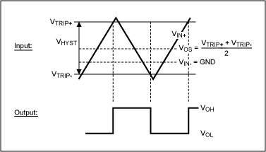
Figure 1. Switching threshold, hysteresis, and offset voltage
The input voltage switching point of a comparator without hysteresis is the input offset voltage, not the zero voltage of the ideal comparator. The offset voltage (that is, the switching voltage) generally changes with changes in temperature and power supply voltage. The power supply rejection ratio (PSRR) is usually used to measure this effect, which represents the effect of the change in nominal voltage on the offset voltage.
The input impedance of an ideal comparator is infinite, so theoretically, it has no effect on the input signal, but the actual input impedance of the comparator cannot be infinite. There is current at the input that passes through the internal resistance of the signal source and flows into the comparator, resulting in Extra pressure difference. Bias current (IBIAS) is defined as the median of the input currents of the two comparators and is used to measure the effect of input impedance. For example, the maximum bias current of the MAX917 and MAX9117 series comparators over the entire operating temperature range is only 2nA. At room temperature (TA = + 25 ° C), the bias current is less than 1nA, as shown in Table 3.
Table 3. Low IBIAS
With the popularization of low-voltage applications, in order to further optimize the working voltage range of the comparator, Maxim uses the structure of npn tube and pnp tube in parallel as the input stage of the comparator, so that the input voltage of the comparator can be expanded to The voltage is 250mV higher, thus reaching the so-called super power swing standard. The input of this comparator allows a larger common-mode voltage. Comparator output Because the comparator has only two different output states, zero level or power supply voltage, the output stage of the comparator with full power swing is an emitter follower, which makes its output signal and power swing There is only a very small pressure difference. This voltage difference depends on the voltage between the collector and the emitter of the comparator when the transistor is saturated. The output voltage of the CMOS rail-to-rail comparator depends on the MOSFET in saturation. Compared with the bipolar transistor structure, the voltage is closer to the power supply voltage under light load.
The output delay time is a key parameter for selecting the comparator. The delay time includes the transmission delay generated by the signal through the components and the rise and fall times of the signal. For high-speed comparators, such as MAX961, MAX9010-MAX9013, the typical value of the delay time Reached 4.5ns and 5ns respectively, and the rise time was 2.3ns and 3ns (note: the measurement of the propagation delay includes the rise time). When designing, it is necessary to pay attention to the influence of different factors on the delay time (Figure 2), including temperature, capacitive load, input overdrive and other factors. For the inverting input, the transmission delay is represented by tPD-; for the non-inverting input, the transmission delay is represented by tPD +. The difference between TPD + and tPD- is called deviation. The power supply voltage also has a large influence on the transmission delay.
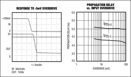
Figure 2. Impact of external factors on transmission delay
Some applications need to balance the speed and power consumption of the comparator. Maxim provides a variety of chip types for this problem, including from the MAX919 with a power consumption of 800nA and a delay time of 30µs to the 6µA power consumption and a delay time of 540ns. MAX9075; MAX998 with power consumption of 600µA, delay time of 20ns to MAX961 with power consumption of 11mA and delay time of 4.5ns; From MAX9107 with power consumption of 350µA and transmission delay of 25ns to MAX9107 with power consumption of 900µA and transmission delay of 5ns The MAX9010 (SC70 package) has a delay time as low as 5ns and the supply current is only 900µA, which provides more choices for product design.
For ultra-high-speed, ECL or PECL output, 500ps delay comparator, please refer to MAX9600 / MAX9601 / MAX9602. The actual comparator is usually used to compare an input voltage and a fixed voltage reference. To meet the needs of this application, Maxim integrates the reference source and the comparator in the same chip, which not only saves space but also consumes less power than an external reference. For example, the maximum current consumption of the MAX9117 in the full temperature range is only 1.3µA (including its internal quasi-source). Considering the change of ambient temperature and the type of reference source, the accuracy of the integrated reference source is generally between 1% and 4%. For applications with higher accuracy requirements, you can consider the MAX9040 series of products, the initial accuracy of the built-in reference source can reach 0.4%, and the maximum temperature drift is 30ppm / ° C.
The dual comparators MAX9017 / MAX9018, MAX923, MAX933 and the open-drain output MAX973 and MAX983 are very suitable for window comparator applications. The internal reference can be connected to the non-inverting or inverting input of these comparators. Overvoltage and undervoltage thresholds can be set (shown in Figure 1). In addition, these chips also contain a hysteresis input pin, which is connected to two voltage divider resistors to set the hysteresis voltage threshold. For ease of use, some comparators (for example: MAX912 / MAX913) also provide complementary outputs, that is, corresponding to changes in the input, two outputs with opposite directions of change.
The fast delay (typical delay time of 1ms during 5mV overdrive) makes the MAX9201 / MAX9203 ideal for high-speed ADCs and high-speed sampling circuits, such as receivers, V / F converters, and other data identification systems.
Other high-speed, low-power comparators, such as the MAX9107 / MAX9108 / MAX9109, are low-cost upgrade products such as the industry standard comparators MAX907 / MAX908 / MAX909. The dual comparator, MAX9107, is available in an 8-pin SOT23 package; the single comparator, MAX9109, is available in a space-saving 6-pin SC70 package; the four-comparator, MAX9108, is available in a 14-pin TSSOP package, see Table 4 and Figure 3.
Table 4. Ultra-high-speed comparator
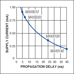
Figure 3. SC70 package, comparator selection application with the best speed / power ratio. This section introduces the typical applications of the three comparators.
The first example is a level shifter, which can complete the conversion from 3V logic to 5V logic. As shown in Figure 4, an open-drain output comparator, such as the MAX986, provides a very simple implementation solution. Similarly, if the comparator supply voltage is allowed (such as the MAX972), it can also implement ± 5V bipolar logic to 3V single Level shift of polarity logic. In the specific application, it should be noted that the input signal should not exceed the swing of the power supply voltage, and the current flowing into the output terminal is limited by a large-value pull-up resistor (refer to Absolute Maximum RaTIngs in MAX986 data sheet).
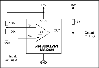
Figure 4. 3V to 5V level shifter
The circuit in Figure 5 solves another common problem. This circuit can convert a bipolar input (in this case, a sine wave) to a unipolar square wave output with an applied bias voltage of:
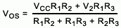
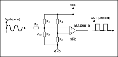
Figure 5. Unipolar comparators handle bipolar signals
Two resistors with the same resistance (R4) set the comparator switching detection threshold at half of the power supply voltage. Figure 6 shows the use of four comparators to form a current detection circuit, which can be used to indicate the four ranges of input current. The bypass resistor is used to convert the input current into a voltage signal. R1-R2 are used to set the gain of the operational amplifier. And provide the required reference voltage for the comparator. R4-R7 are used to set the detection threshold corresponding to different digital output states.
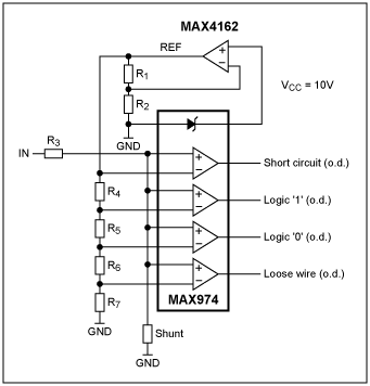
Figure 6. Scheme for measuring four current ranges
For a long time, due to the influence of operational amplifiers, the application of comparators has not been given due attention. Until now, with the improvement of the performance index of the comparator, making it better for the basic task of voltage comparison, this situation has been improved. This article mainly introduces the performance of the new comparator and its typical applications. Function of the comparator The two inputs of the comparator are analog signals, and the output is a binary signal. When the difference of the input voltage increases or decreases, the output remains constant. From this perspective, the comparator can also be used as a 1-bit analog-to-digital converter (ADC). Comparator and Operational Amplifier Operational amplifier can be used as a comparator in principle when negative feedback is not added, but because the open-loop gain of the operational amplifier is very high, it can only handle signals with very small input differential voltage. Moreover, in this case, the response time of the operational amplifier is much slower than the comparator, and it also lacks some special functions, such as hysteresis, internal reference, etc.
Comparators cannot usually be used as op amps. Comparators can be adjusted to provide a very small time delay, but their frequency response characteristics are limited. Op amps take advantage of frequency response correction and become a flexible and versatile device. In addition, many comparators also have internal hysteresis circuits, which avoids output oscillations, but at the same time makes them unusable as operational amplifiers. The power supply voltage comparator and the operational amplifier work at the same power supply voltage. The traditional comparator requires a dual power supply such as ± 15V or a single power supply up to 36V. These products are still in demand in industrial control, and many manufacturers are still providing this. Products.
However, from the market development trend, most of the current applications require the comparator to work within the single power supply voltage range allowed by the battery voltage. Furthermore, the comparator must have a low current and a small package. . For example, the MAX919, MAX9119, and MAX9019 comparators can operate in the voltage range of 1.6V or 1.8V to 5.5V. The maximum sink current in the full temperature range is only 1.2µA / 1.5µA. They are available in SOT23, SC70 packages, similar to the MAX965 and The working voltage of the MAX9100 comparator can be as low as 1.6V or even 1.0V, so it is very suitable for battery-powered portable products, see Table 1.
Table 1. Selection guide for MAX9015-MAX9020
| Part | Comparator (s) | Int. Reference (V) | Output | Supply Current (µA) |
| MAX9015A | 1 | 1.236, ± 1% | Push-pull | 1 |
| MAX9016A | 1 | 1.236, ± 1% | Open drain | 1 |
| MAX9017A | 2 | 1.236, ± 1% | Push-pull | 1.2 |
| MAX9017B | 2 | 1.24, ± 1.75% | Push-pull | 1.2 |
| MAX9018A | 2 | 1.236, ± 1% | Open drain | 1.2 |
| MAX9018B | 2 | 1.24, ± 1.75% | Open drain | 1.2 |
| MAX9019 | 2 | - | Push-pull | 0.85 |
| MAX90120 | 2 | - | Open drain | 0.85 |
Table 2. Comparators in tiny packages
| Package | Part | Comparator (s) | Int. Reference | Output | Supply Current (µA) |
| 6-UCSP | MAX9025 | 1 | Push-pull | 1.0 | |
| 6-UCSP | MAX9026 | 1 | Open drain | 1.0 | |
| 6-UCSP | MAX9027 | 1 | Push-pull | 0.6 | |
| 6-UCSP | MAX9028 | 1 | Open drain | 0.6 | |
| 5-SC70 | MAX9117 | 1 | Push-pull | 0.6 | |
| 5-SC70 | MAX9118 | 1 | Open drain | 0.6 | |
| 5-SC70 | MAX9119 | 1 | Push-pull | 0.35 | |
| 5-SC70 | MAX9120 | 1 | Open drain | 0.35 |
Figure 1. Switching threshold, hysteresis, and offset voltage
The input voltage switching point of a comparator without hysteresis is the input offset voltage, not the zero voltage of the ideal comparator. The offset voltage (that is, the switching voltage) generally changes with changes in temperature and power supply voltage. The power supply rejection ratio (PSRR) is usually used to measure this effect, which represents the effect of the change in nominal voltage on the offset voltage.
The input impedance of an ideal comparator is infinite, so theoretically, it has no effect on the input signal, but the actual input impedance of the comparator cannot be infinite. There is current at the input that passes through the internal resistance of the signal source and flows into the comparator, resulting in Extra pressure difference. Bias current (IBIAS) is defined as the median of the input currents of the two comparators and is used to measure the effect of input impedance. For example, the maximum bias current of the MAX917 and MAX9117 series comparators over the entire operating temperature range is only 2nA. At room temperature (TA = + 25 ° C), the bias current is less than 1nA, as shown in Table 3.
Table 3. Low IBIAS
| Part | IBIAS |
| MAX9025—MAX9028 | 1nA (max) @ TA = + 25 ° C 2nA (max) @ TA = TMIN to TMAX |
| MAX9117—MAX9120 | 1nA (max) @ TA = + 25 ° C 2nA (max) @ TA = TMIN to TMAX |
| MAX917 | 1nA (max) @ TA = + 25 ° C 2nA (max) @ TA = TMIN to TMAX |
With the popularization of low-voltage applications, in order to further optimize the working voltage range of the comparator, Maxim uses the structure of npn tube and pnp tube in parallel as the input stage of the comparator, so that the input voltage of the comparator can be expanded to The voltage is 250mV higher, thus reaching the so-called super power swing standard. The input of this comparator allows a larger common-mode voltage. Comparator output Because the comparator has only two different output states, zero level or power supply voltage, the output stage of the comparator with full power swing is an emitter follower, which makes its output signal and power swing There is only a very small pressure difference. This voltage difference depends on the voltage between the collector and the emitter of the comparator when the transistor is saturated. The output voltage of the CMOS rail-to-rail comparator depends on the MOSFET in saturation. Compared with the bipolar transistor structure, the voltage is closer to the power supply voltage under light load.
The output delay time is a key parameter for selecting the comparator. The delay time includes the transmission delay generated by the signal through the components and the rise and fall times of the signal. For high-speed comparators, such as MAX961, MAX9010-MAX9013, the typical value of the delay time Reached 4.5ns and 5ns respectively, and the rise time was 2.3ns and 3ns (note: the measurement of the propagation delay includes the rise time). When designing, it is necessary to pay attention to the influence of different factors on the delay time (Figure 2), including temperature, capacitive load, input overdrive and other factors. For the inverting input, the transmission delay is represented by tPD-; for the non-inverting input, the transmission delay is represented by tPD +. The difference between TPD + and tPD- is called deviation. The power supply voltage also has a large influence on the transmission delay.
Figure 2. Impact of external factors on transmission delay
Some applications need to balance the speed and power consumption of the comparator. Maxim provides a variety of chip types for this problem, including from the MAX919 with a power consumption of 800nA and a delay time of 30µs to the 6µA power consumption and a delay time of 540ns. MAX9075; MAX998 with power consumption of 600µA, delay time of 20ns to MAX961 with power consumption of 11mA and delay time of 4.5ns; From MAX9107 with power consumption of 350µA and transmission delay of 25ns to MAX9107 with power consumption of 900µA and transmission delay of 5ns The MAX9010 (SC70 package) has a delay time as low as 5ns and the supply current is only 900µA, which provides more choices for product design.
For ultra-high-speed, ECL or PECL output, 500ps delay comparator, please refer to MAX9600 / MAX9601 / MAX9602. The actual comparator is usually used to compare an input voltage and a fixed voltage reference. To meet the needs of this application, Maxim integrates the reference source and the comparator in the same chip, which not only saves space but also consumes less power than an external reference. For example, the maximum current consumption of the MAX9117 in the full temperature range is only 1.3µA (including its internal quasi-source). Considering the change of ambient temperature and the type of reference source, the accuracy of the integrated reference source is generally between 1% and 4%. For applications with higher accuracy requirements, you can consider the MAX9040 series of products, the initial accuracy of the built-in reference source can reach 0.4%, and the maximum temperature drift is 30ppm / ° C.
The dual comparators MAX9017 / MAX9018, MAX923, MAX933 and the open-drain output MAX973 and MAX983 are very suitable for window comparator applications. The internal reference can be connected to the non-inverting or inverting input of these comparators. Overvoltage and undervoltage thresholds can be set (shown in Figure 1). In addition, these chips also contain a hysteresis input pin, which is connected to two voltage divider resistors to set the hysteresis voltage threshold. For ease of use, some comparators (for example: MAX912 / MAX913) also provide complementary outputs, that is, corresponding to changes in the input, two outputs with opposite directions of change.
The fast delay (typical delay time of 1ms during 5mV overdrive) makes the MAX9201 / MAX9203 ideal for high-speed ADCs and high-speed sampling circuits, such as receivers, V / F converters, and other data identification systems.
Other high-speed, low-power comparators, such as the MAX9107 / MAX9108 / MAX9109, are low-cost upgrade products such as the industry standard comparators MAX907 / MAX908 / MAX909. The dual comparator, MAX9107, is available in an 8-pin SOT23 package; the single comparator, MAX9109, is available in a space-saving 6-pin SC70 package; the four-comparator, MAX9108, is available in a 14-pin TSSOP package, see Table 4 and Figure 3.
Table 4. Ultra-high-speed comparator
| Speed ​​(ns) | Part | Comparator (s) | Supply Current (A) | Package |
| 4.5 | MAX999 | 1 | 5m | 5-SOT23 |
| 4.5 | MAX962 | 2 | 5m | 8-µMAX |
| 5 | MAX9010 | 1 | 0.9m | 6-SC70 |
| 5 | MAX9011 | 1 | 0.9m | 6-SOT23 |
| 5 | MAX9012 | 2 | 0.9m | 8-µMAX |
| 5 | MAX9013 | 1 | 0.9m | 8-µMAX |
| 7 | MAX9201 | 4 | 4.7m | 16-TSSOP |
| 7 | MAX9202 | 2 | 2.5m | 14-TSSOP |
| 7 | MAX9203 | 1 | 1.3m | 8-SOT23 |
| 8 | MAX900 | 4 | 2.5m | 20-SO |
| 8 | MAX901 | 4 | 2.5m | 16-SO |
| 8 | MAX902 | 2 | 2.5m | 14-SO |
| 8 | MAX903 | 1 | 2.5m | 8-SO |
| 10 | MAX912 | 2 | 6m | 16-SO |
| 10 | MAX913 | 1 | 6m | 8-µMAX |
| 25 | MAX9107 | 2 | 350µ | 8-SOT23 |
| 25 | MAX9108 | 4 | 350µ | 14-TSSOP |
| 25 | MAX9109 | 1 | 350µ | 6-SC70 |
| 40 | MAX9140 | 1 | 150µ | 5-SC70 |
| 40 | MAX9141 | 1 | 165µ | 8-SOT23 |
| 40 | MAX9142 | 2 | 150µ | 8-SOT23 |
| 40 | MAX9144 | 4 | 150µ | 14-TSSOP |
| 40 | MAX907 | 2 | 700µ | 8-SO |
| 40 | MAX908 | 4 | 700µ | 14-SO |
Figure 3. SC70 package, comparator selection application with the best speed / power ratio. This section introduces the typical applications of the three comparators.
The first example is a level shifter, which can complete the conversion from 3V logic to 5V logic. As shown in Figure 4, an open-drain output comparator, such as the MAX986, provides a very simple implementation solution. Similarly, if the comparator supply voltage is allowed (such as the MAX972), it can also implement ± 5V bipolar logic to 3V single Level shift of polarity logic. In the specific application, it should be noted that the input signal should not exceed the swing of the power supply voltage, and the current flowing into the output terminal is limited by a large-value pull-up resistor (refer to Absolute Maximum RaTIngs in MAX986 data sheet).
Figure 4. 3V to 5V level shifter
The circuit in Figure 5 solves another common problem. This circuit can convert a bipolar input (in this case, a sine wave) to a unipolar square wave output with an applied bias voltage of:
Figure 5. Unipolar comparators handle bipolar signals
Two resistors with the same resistance (R4) set the comparator switching detection threshold at half of the power supply voltage. Figure 6 shows the use of four comparators to form a current detection circuit, which can be used to indicate the four ranges of input current. The bypass resistor is used to convert the input current into a voltage signal. R1-R2 are used to set the gain of the operational amplifier. And provide the required reference voltage for the comparator. R4-R7 are used to set the detection threshold corresponding to different digital output states.
Figure 6. Scheme for measuring four current ranges
Children Toy Car,Kids Electric Cars,Mini Cars For Kids,Toy Cars For Toddlers
Jinan Huajiang environmental protection and energy saving Technology Co., Ltd , https://www.hjnewenergy.com