Design of Current-Fieldbus Conversion Instrument Based on WORLDFIP
Discuss the development of current-fieldbus converter based on WorldFIP fieldbus protocol. The principle and specific design of the current-field bus converter are specifically introduced from two aspects of hardware design and software development.
Keywords: converter; protocol; FOUNDATION fieldbus
1.1 The input module is shown in Figure 2. In order to save costs and fully improve the conversion efficiency of the IF, the IF is designed to have four input conversion channels. The function of connecting a resistor to each input end is to multiply the input signal with a correct gain to suit the signal reception range of the A / D converter. The input is an analog signal of 4 ~ 20mA. After a resistance of R = 100Ω, the signal entering the A / D converter is a voltage signal of 0.4 ~ 2V (the standard voltage of ADS1110 is 2.048V).

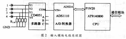
The role of power isolation and signal isolation is to prevent the input signal from forming a loop with ground and introducing interference. The control signal from the CPU of the main circuit board and the signal from the A / D converter are transmitted through the photocoupler, thereby realizing the isolation of the signal ground.
The central processing unit CPU is the core component of the current-field bus, which controls the coordination, linearization and communication of the various components of the entire instrument. The CPU uses AT91M40800. The chip integrates ARM7TDMI core, with high-performance 32-bit RISC; on-chip SRAM and ROM; 4G linear address space, 32-bit programmable I / O lines and other characteristics. In addition, the on-chip JTAG debugging port of this series of single chip can be emulated online. The system program is stored in the PROM outside the CPU, the operation data is temporarily stored in the RAM, and some important application programs such as calibration, configuration and identification are stored in the EEPROM. The EEPROM memory on the main circuit board is used to store the configuration parameters (referring to the parameters of the function module).
1.2 WorldFIP communication module In the design of the communication module, the communication unit adopts the WorldFIP communication microcontroller MICROFIP designed by ALSTOM, and the communication interface part uses the WorldFIP bus driver FIELDDRIVE and WorldFIP isolation transformer F IELDTR designed by ALSTOM. The composition block diagram of the communication card is shown in Figure 3. ?
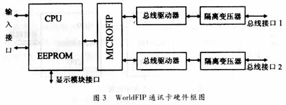
1) Physical layer service: choose between EN10570 and FIP standards; 2) Data link layer service: variable transmission service and message transmission service; 3) network management service: MICROFIP media redundancy management; 4) additional functions: Input / output port, get the station address through the parallel port.
FIELDRIVE components are a set of fully integrated bus driver circuits used to provide the interface between protocol components and field bus isolation transformers. It integrates a bus driver, a bus receiver, a set of transmission error detection circuits, a monitoring interface . The FIELDTR element provides electrical isolation between the FIELDDRIVE bus driver and the physical media of the fieldbus.
1.3 The display panel uses the character LCD dot matrix module HD44780, which can display 5 × 7 dot font 192 characters, 5 × 10 dot font 32 characters, and can be self-programmed 8 (5 × 7 dots) or 4 (5 × 10 dots) ) Kinds of characters. The command function of this module is strong, and can be combined into various input, display, shift modes to meet different requirements. The interface has 8 × 8bitRAM. ?
 ?
? This Computer Speaker is powered by USB interface on computers or laptops, plug and play, save energy. 3W output brings you high-quality clear binaural sound. Lightweight and portable design makes you can hold it with single hand, save space on the desk. Made of ABS and TPU, which makes this speaker durable and firm. Believe it is a great companion for your computer and laptop.

Computer Speaker
Usb Powered Speaker,Usb Small Speakers,Mini Portable Speakers,Desktop Mini Speakers
SHENZHEN HONK ELECTRONIC CO., LTD , https://www.honktech.com