Despite the widespread use of digital electronics, the real world is sTIll analog. As a result, digital-to-analog converters (DACs) are needed at the point of contact between digital and analog sections of a system. The following discussion covers important parameters that should be taken into account when selecting a DAC, and it also highlights some interesting features available in new devices.
Most electronic devices now include digital control circuitry (as illustrated by the recent Y2K problem), but analog values ​​are still needed to control valves, loudspeakers, and other actuators. The conversion from digital to analog is usually accomplished within a dedicated D / A converter . This DAC can be selected from the vast array of available standard circuits, in accordance with the conversion requirements and system settings.
ResolutionIn selecting a DAC, the first step is to determine the necessary resolution N, where 2N least significant bits (LSBs) equals the maximum analog output. The market offers greatest product variety for DACs that specify a resolution in the range 8 to 16-bits (256 to 65,536 steps). Resolution gives no indication of accuracy, however, because other sources of error must be taken into account.
The next parameter of interest is integral nonlinearity (INL), which describes the deviation of a DAC's transfer function from a straight line. For DACs, this deviation is measured at every step (Figure 1a). The straight line can be a best approximation to the actual transfer function, or a line drawn between the transfer function's end points (after subtracting the gain and offset errors). Though low-cost devices specify this parameter as high as ± 16LSBs, it can often be improved through the use of correction coefficients in the operation software. For high-end DACs, INL values ​​are better than ± 1LSB.
Differential nonlinearity (DNL) is the difference between an actual step height and the ideal value of 1LSB. The target value for DNL (<1LSB) ensures that the DAC is monotonic. This means no data is lost because the output always changes in accord with the digital input; it increases in response to a digital increment, and decreases in response to a digital decrement. Figure 1b defines DNL in terms of the transfer function.
The deviation of the actual output from the ideal value is graphed in Figure 1c. For DACs, offset error equals the output voltage when the digital input is zero. This error remains constant for all input values, and normally can be compensated by calibrating the circuit . Offset error is often specified as an absolute value in millivolts rather than LSBs. (Offset error in LSBs depends on the output step height, which in turn depends on the level of reference voltage.) An acceptable offset error is usually less than ± 10mV .
Gain error is defined as the difference between the ideal maximum output voltage and the actual maximum value of the transfer function after subtracting the offset error (Figure 1d). Because gain error changes the slope of the transfer function, it delivers the same percentage error for each step. Gain error is expressed in LSB or millivolts, as a percent of the maximum value.
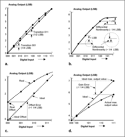
Figure 1. These graphs define major performance parameters for a DAC: integral nonlinearity (a), differential nonlinearity (b), offset error (c), and gain error (d). Dynamic Output Characteristics An ideal DAC would deliver its analog output immediately after a digital value is applied to the input. Actual DACs, however, impose a settling time that consists of the internal propagation delay and a limited slew rate in the output driver. Settling time begins with the start of a conversion, ends when the DAC output becomes stable, and includes any static error.
A type of noise called digital feedthrough can be measured at the output of a DAC. Every digital transition at the input couples through to the output. Though caused by the DAC itself, this effect is made worse by improper grounding and board layout.
Data InterfaceFormerly, the most widely used data interface was the parallel type. It still offers the advantage of fast transmission and a simple data protocol. The lower pin count of a serial interface, on the other hand, requires less board space and allows a smaller package. The SPI and related types, which require simpler handling by the IC manufacturer and the user, have a much larger market share than does the 2-wire I²C-compatible interface.
SPI is a 3-wire interface (data input, data output, and clock) that also requires a chip-select wire for device addressing. Because galvanic isolation of the signal path is often required as well, the unidirectional data lines of a 3- wire interface offer yet another advantage (isolation of unidirectional lines is easily implemented with optocouplers). New DACs like the 12-bit MAX5539 and the MAX5543 integrate this isolation within the package, thereby easing the design of analog data outputs in industrial equipment.
Reference Voltage To a large extent, the characteristics of a DAC are defined by its reference voltage, whether generated within the DAC or applied externally. First, the reference voltage (VREF) sets the DAC's maximum output voltage if the output signal is not amplified by an additional output stage. VREF also defines the voltage step by which the output changes in response to a 1-LSB transition at the input. One step equals VREF / 2N, where N is the DAC resolution.
At a constant temperature, the output voltage of a reference varies within a range specified by its initial accuracy. For a changing temperature, the output voltage drift has a direct bearing on the DAC's quality (Table 1).
Table 1. Allowable Temperature Range for Maximum Drift of ± 1LSB in 2.5V References
| Resolution (bit) | Step Count | 1 LSB at 2.5V (mV) | Max. Temperature Drift (ppm / ° C) at 0 ... 70 ° C | Max. Temperature Drift (ppm / ° C) at -40 ... 85 ° C |
| 8 | 256 | 9,766 | 111,61 | 62,50 |
| 10 | 1024 | 2,441 | 27,90 | 15,63 |
| 12 | 4096 | 0,610 | 6,98 | 3,91 |
| 13 | 8192 | 0,305 | 3,49 | 1,95 |
| 14 | 16384 | 0,153 | 1,74 | 0,98 |
| 16 | 65536 | 0,038 | 0,44 | 0,24 |
Table 1 makes obvious that a DAC requires minimum drift in its reference. Integrated references are typically 100ppm / ° C, and are therefore qualified only for a limited temperature range. An exception is the 12- / 13-bit MAX5122 / MAX5132, whose integrated precision reference specifies a maximum drift of 10ppm / ° C (3ppm / ° C typically).
When connecting an external reference, you should consider not only the current required and the voltage range of the DAC's reference input, but also any dynamic effects produced by the DAC's inner structure. With variation of the applied digital value, the reference input resistance can also change. Thus, the reference selected must be capable of following each load step within the required time, or you must add a capacitor or an op-amp buffer.
DACs with an external reference input (like the MAX5170) can also be operated in the multiplying mode. A variable voltage (rather than a constant one) is applied to the reference input (Figure 2). The variable voltage is multiplied with the adjusted digital input value and transferred to the output, producing the effect of an accurate digital potentiometer. For this operating mode you should consider the DAC's bandwidth and voltage range, as well as dynamic characteristics of the reference input; such as voltage feedthrough from the reference input to the output at a digital value of zero.
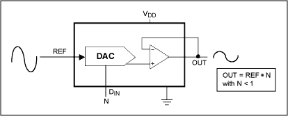
Figure 2. A multiplying DAC produces the product of the digital input and an AC-reference signal.
Output StagesThe output stage of a DAC can be designed to provide a voltage output or a current output, but the simpler voltage output has a much larger market share. Some Maxim devices offer a voltage output with fixed gain or an uncommitted amplifier as options, the so-called "force-sense" outputs. That arrangement lets you set an individual gain with two external resistors (Figure 3a). The force-sense voltage output also lets you realize a current output (Figure 3b).
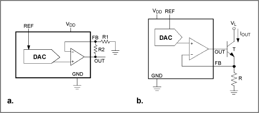
Figure 3. An uncommitted output op amp provides a "force-sense" output (a). Configured as shown in (b), the op amp provides a current output for the DAC.
The MAX5120 / MAX5170 family provides a special power-up feature called glitch prevention. Without this feature, the DAC output simply follows the supply voltage at power-up until the integrated circuits start to work. That action corrupts the output with an impulse up to 3V high, which can lead to a malfunction in the following circuitry. MAX5120 / MAX5170 devices suppress this impulse. They also deliver a power-up reset that clears all DAC registers. This reset can be adjusted for power-up at 0V or at half of the maximum output voltage (midrange), as is required for bipolar output stages.
Most new devices operate on a unipolar power supply, but they can deliver bipolar output signals if you add an external bipolar amplifier and define midrange of the maximum output voltage as zero. Parts like the 12-bit MAX530 operate on bipolar supplies and deliver bipolar output voltages directly. As another consideration for the DAC power supply, you should note that latch-up can occur if a digital-input voltage is 0.3V higher then the supply voltage. In particular, data signals should not be applied to the DAC input at power-up or power-down. Schottky diodes provide protection against this problem (Figure 4).
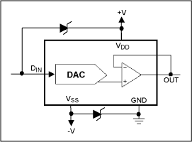
Figure 4. Schottky diodes provide protection against latch-up effects at power-up or power-down.
A similar version of this article appeared in the June 2001 issue of EPD magazine.
Win 3 Cap Lamps are produced under IECEX quality control. The lamps are applied with IECEX explosive-proof certificates, build with brilliant electronic design and superior impact resistant, explosion-proof housing material, It is completely static proof and fire resistan.
The high quality LED has a lifespan of more than 30,000 hours and the phosphate technology battery up to 1000 cycles.
Small size and light weight, easy to carry
The highest ingress protection IP 68
Various application: coal miners, tunnel projects, oil fielda , camping, hiking, night fishing, night flying, sailing, etc.
Static Proof Cap Lamp Fire Resistant
Miners Lights For Hard Hats,Underground Mining Lights,Cordless Led Mining Cap Lights,Coal Miners Hard Hat With Light
ZHEJIANG HUACAI OPTIC-TECHNOLOGY CO LTD , https://www.win3safety.com